

Semiconductor Power Conversion Apparatus
a technology of power conversion apparatus and semiconductor, which is applied in the direction of power conversion system, pulse technique, electronic switching, etc., can solve the problems of difficult to locate the charging current supply circuit close to the igbt, and the charge current supply circuit is difficult to charge current supply circuit, so as to reduce the number of clamping elements
- Summary
- Abstract
- Description
- Claims
- Application Information
AI Technical Summary
Benefits of technology
Problems solved by technology
Method used
Image

Examples
embodiment 1
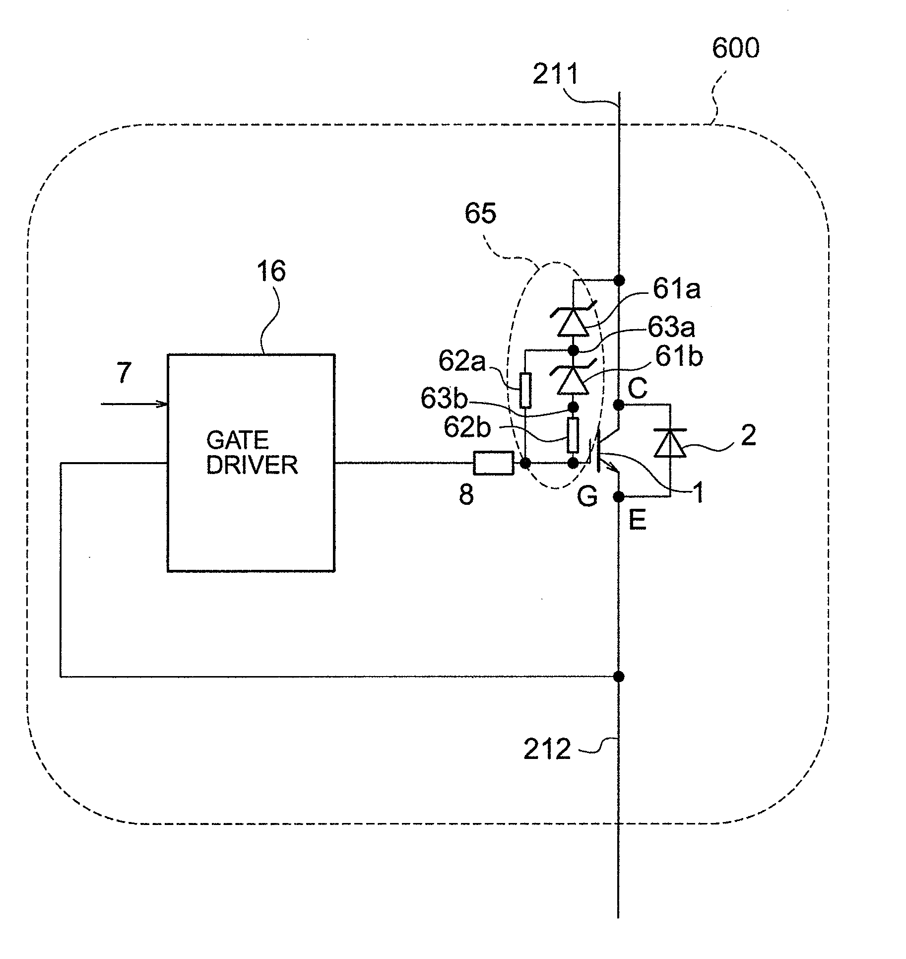
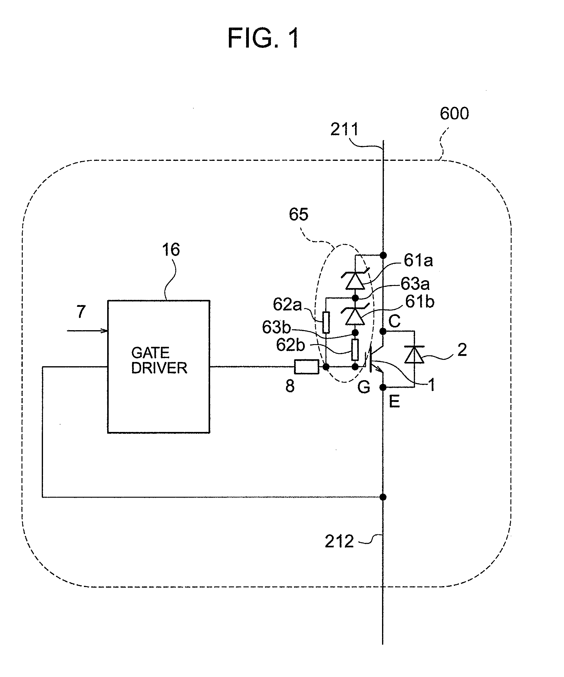
[0026] Explanation will be made first as to the arrangement of an IGBT power conversion apparatus in accordance with an embodiment with use of FIGS. 1 and 5. FIG. 5 shows a major part of the power conversion apparatus to which the present invention is applied, and FIG. 1 shows a major part of an arm 20 in FIG. 5.
[0027] First of all, the arrangement of the power conversion apparatus according to a first embodiment will be explained by referring to FIG. 5. In the power conversion apparatus of the present embodiment, 3 of two arms 20 connected in series are connected in parallel and also connected to a DC voltage source 21 via wiring lines 201 and 202. The wiring has been expressed by wiring lines 201 and 202. However, in order to reduce a parasitic inductance, the arm 20 is usually connected to the DC voltage source 21 via busbars or the like. As the DC voltage source 21, a DC capacitor may be used. Meanwhile, when the power conversion apparatus is an AC-to-DC conversion type, midpoi...
embodiment 2
[0035] A second embodiment will next be explained. The present embodiment is directed to protecting the IGBT 1 from an overvoltage by limiting a current shunted from a clamping element to a gate driver and supplying more gate charging current from the clamping element to the gate of the IGBT 1.
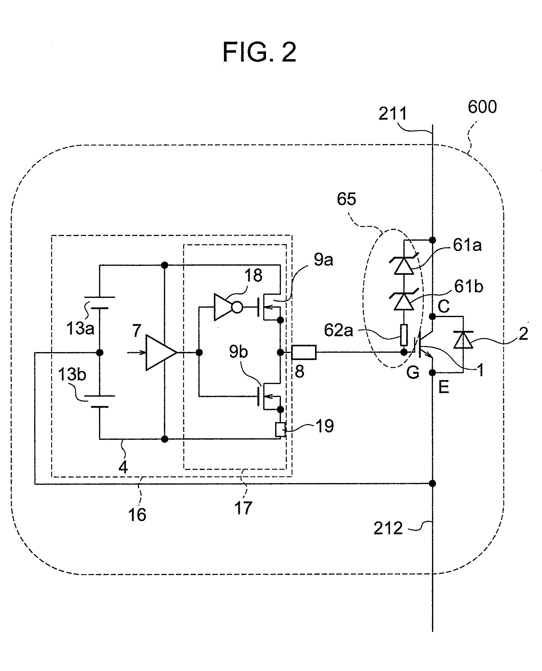
[0036] In the present embodiment, each arm 20 in FIG. 5 has such an arrangement as shown by an IGBT set 600 in FIG. 2. In the second embodiment, a resistor 19 is provided between a MOS FET 9b and a low-voltage side power line 4 of a gate driver 16 in an output stage of the gate driver. When a MOS FET 9a is turned ON and the MOS FET 9b is turned OFF, the gate potential of the IGBT 1 becomes a potential of a high-voltage side power line of the gate driver 16, the gate voltage of the IGBT 1 exceeds a threshold in such a manner that the IGBT is put in its ON state. When the MOS FET 9a is turned OFF and the MOS FET 9b is turned ON, on the other hand, charges are pulled out from the gate of the IGB...
embodiment 3
[0041] Explanation will next be made as to a third embodiment. Even in the present embodiment, a current branched from a clamping element to a gate driver is limited to supply more gate charging current to the gate of an IGBT 1, thus protecting the IGBT 1 from an overvoltage, similarly to the second embodiment.
[0042] In the present embodiment, each arm 20 in FIG. 3 has such an arrangement as shown by the IGBT set 600 in FIG. 2. The third embodiment is featured in that a reactor 28 is connected between an overvoltage protection circuit 65 and a gate driver 16.
[0043] When a MOS FET 9a is turned ON and a MOS FET 9b is turned OFF in an output stage 17 of the gate driver 16, the gate potential of the IGBT 1 is a potential on the high-voltage side power line of the gate driver, the gate voltage of the IGBT 1 exceeds a threshold, whereby the IGBT 1 is put in its ON state. When the MOS FET 9a is turned OFF and the MOS FET 9b is turned ON, on the other hand, charges are pulled out from the...
PUM
 Abstract
Description
Claims
Application Information