

Solid-state imaging device and method for fabricating the same
a technology of solid-state imaging and fabrication methods, which is applied in the direction of semiconductor devices, radio frequency controlled devices, electrical devices, etc., can solve the problem of not being able to substantially reduce the global level difference on the surface of interlayer insulation films, and achieve the effect of higher resolution
- Summary
- Abstract
- Description
- Claims
- Application Information
AI Technical Summary
Benefits of technology
Problems solved by technology
Method used
Image

Examples
first embodiment
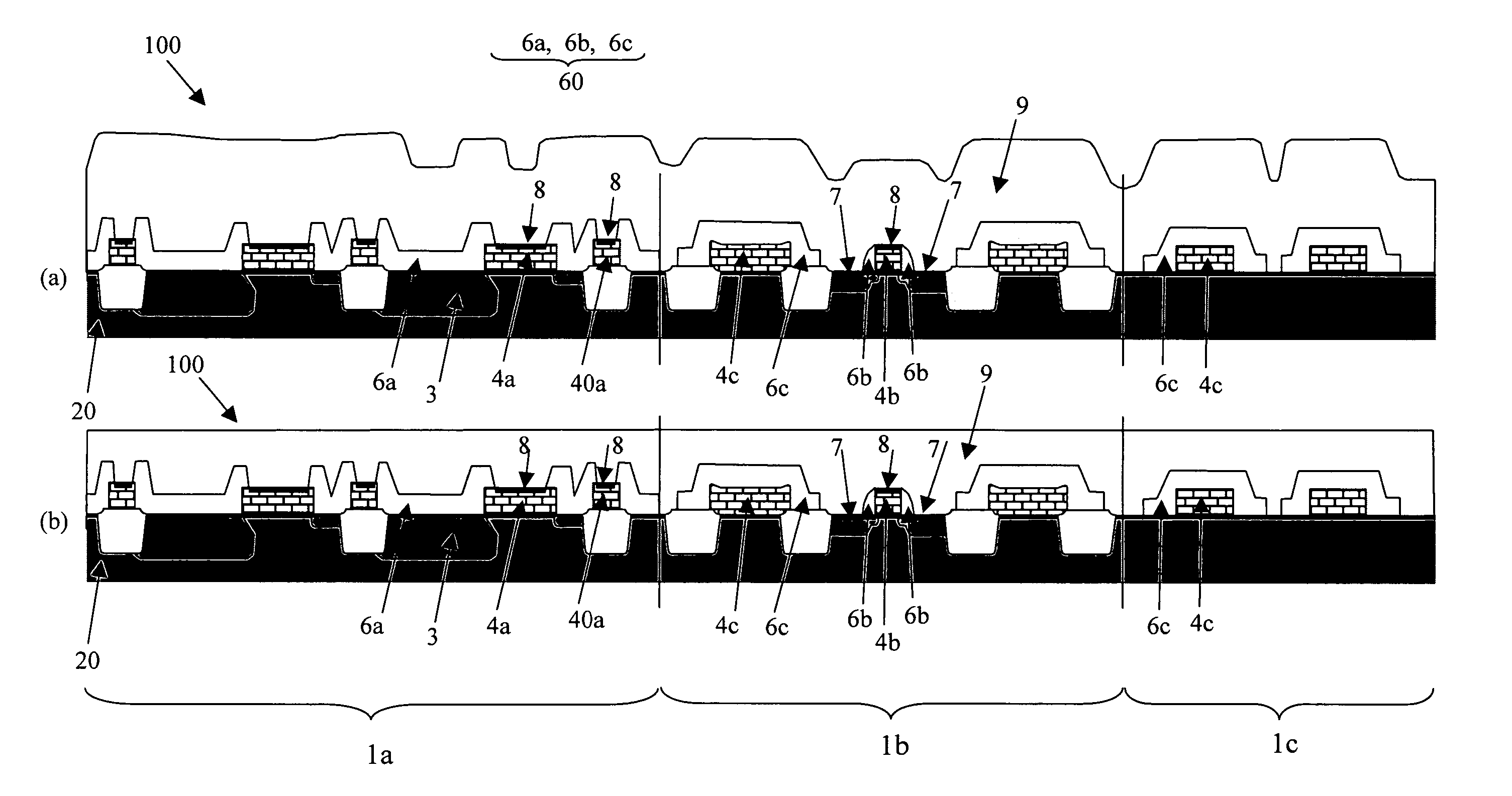
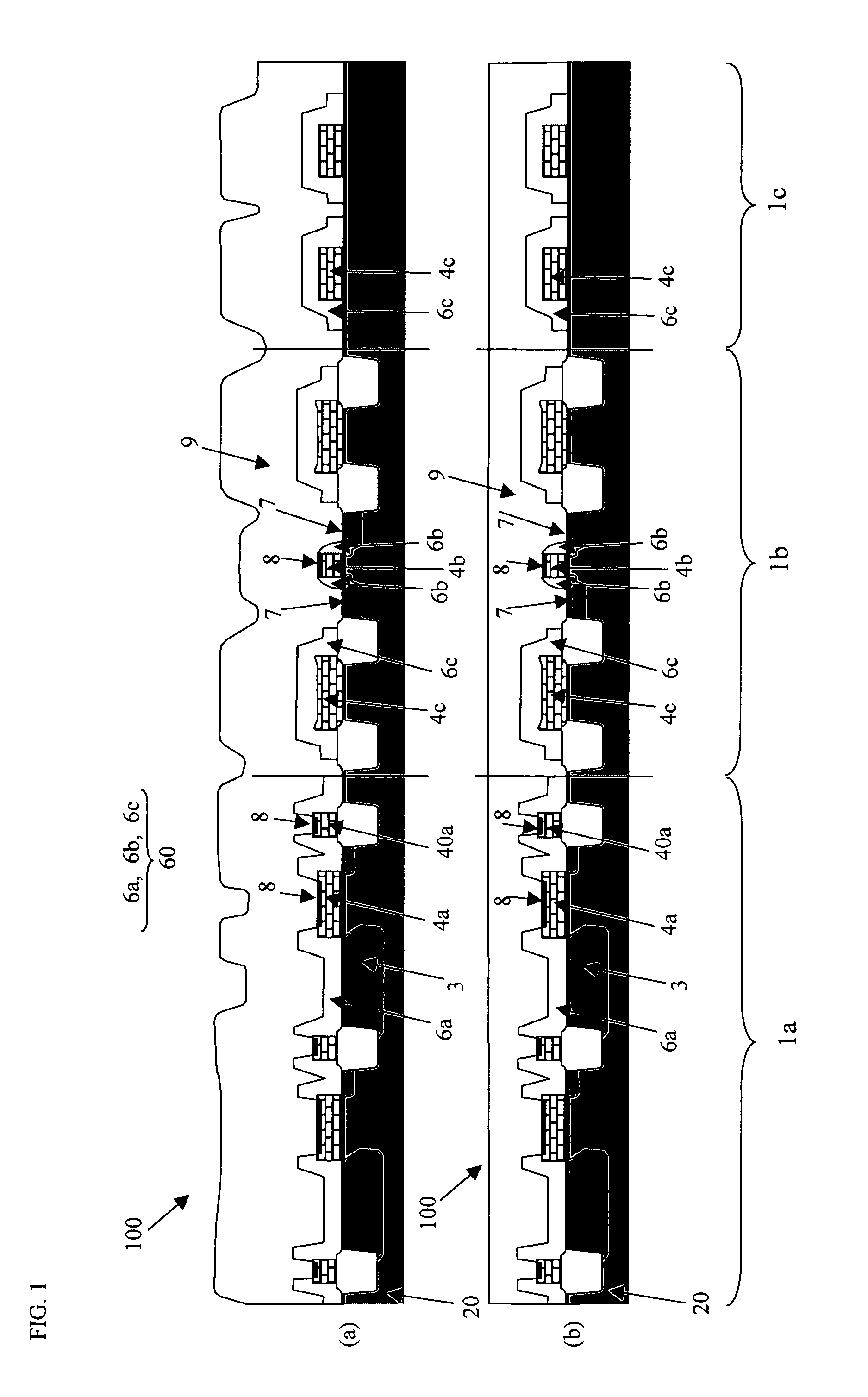
[0045] Hereinafter, a first embodiment of the present invention will be described with reference to the drawings. FIG. 1(b) is a cross-sectional view illustrating a MOS type solid-state imaging device according to the first embodiment. FIG. 1(a) is a cross-sectional view illustrating a state before a CMP is performed on a surface of an interlayer insulation film of the solid-state imaging device shown in FIG. 1(b).
[0046] On a main surface of a semiconductor substrate 20, a solid-state imaging device 100 according to the first embodiment comprises a pixel region lain which pixels are formed, a peripheral circuit region 1b, formed around the periphery of the pixel region, in which driving circuit for driving the pixels included in the pixel region 1a is formed, and a scribe lane region 1c, formed around the periphery of the peripheral circuit region 1b, for separating an integrated circuit region including the pixel region 1a and the peripheral circuit region 1b from an adjacent inte...
second embodiment
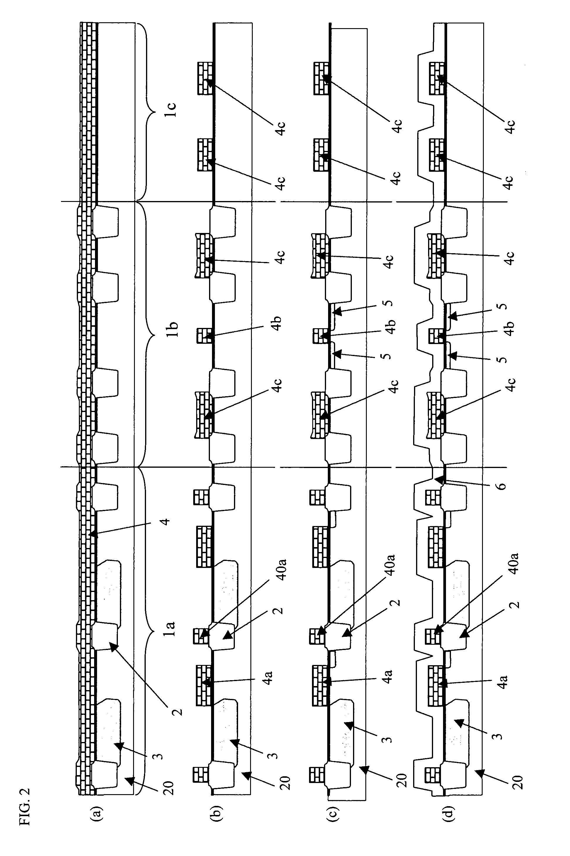
[0066] Hereinafter, a second embodiment of the present invention will be described with reference to the drawings. FIG. 4(b) is a cross-sectional view illustrating the MOS type solid-state imaging device according to the second embodiment. FIG. 4(a) is a cross-sectional view illustrating a state before the CMP is performed on the surface of the interlayer insulation film of the solid-state imaging device shown in FIG. 4(b). In the second embodiment, the same components as those of the first embodiment will be denoted by the same reference numerals.
[0067] On the main surface of the semiconductor substrate 20, a solid-state imaging device 101 according to the second embodiment comprises the pixel region 1a in which the pixels are formed, the peripheral circuit region 1b, formed around the periphery of the pixel region, in which the driving circuit for driving the pixels included in the pixel region 1a is formed, and the scribe lane region 1c, formed around the periphery of the periph...
PUM
 Abstract
Description
Claims
Application Information