Polishing pad and chemical mechanical polishing apparatus comprising the same

a technology of mechanical polishing and polishing pad, which is applied in the direction of grinding machine, manufacturing tools, lapping machines, etc., can solve the problems of variation in the rate at which material is removed across the surface, difficult to planarize a semiconductor substrate sufficiently, and non-uniform distribution of slurry across the surface of the polishing pad. to achieve the effect of enhancing the uniformity of the ra

Inactive Publication Date: 2008-04-17
SAMSUNG ELECTRONICS CO LTD
View PDF7 Cites 15 Cited by
  • Summary
  • Abstract
  • Description
  • Claims
  • Application Information

AI Technical Summary

Benefits of technology

[0009] An object of the present invention is to provide a polishing pad of a chemical mechanical polishing (CMP) apparatus that enhances the uniformity of the rate at which material is removed from a substrate being polished, thereby ensuring the reproducibility of the CMP process.
[0013] A respective slurry hole extends through the pad to the first major groove. Each one minor groove has a closed geometric shape and is connected to the first major groove. Thus, slurry supplied through the slurry hole towards the upper surface of the pad will be fed to the minor groove via the first major groove. Also, the cross-sectional area of each minor groove is smaller than that of the first major groove to thereby regulate the flow of the slurry from the first major groove.

Problems solved by technology

For this reason, the slurry is distributed non-uniformly across the surface of the polishing pad.
Such non-uniform slurry distribution causes variations in the rate at which material is removed across the surface of the semiconductor substrate.
Thus, the conventional polishing pad makes it difficult to planarize a semiconductor substrate sufficiently and to effect a CMP process that is reproducible.

Method used


Image

  • Polishing pad and chemical mechanical polishing apparatus comprising the same
  • Polishing pad and chemical mechanical polishing apparatus comprising the same
  • Polishing pad and chemical mechanical polishing apparatus comprising the same

Examples


first embodiment

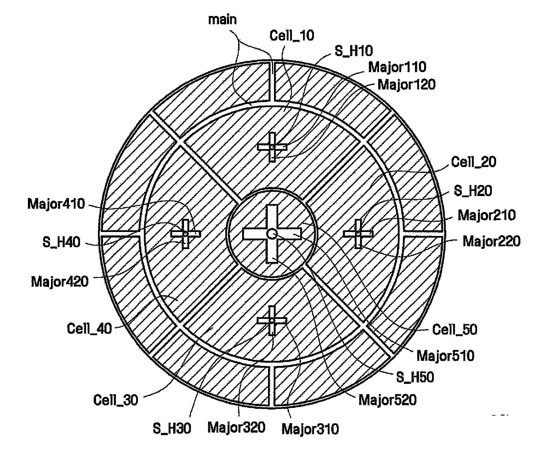
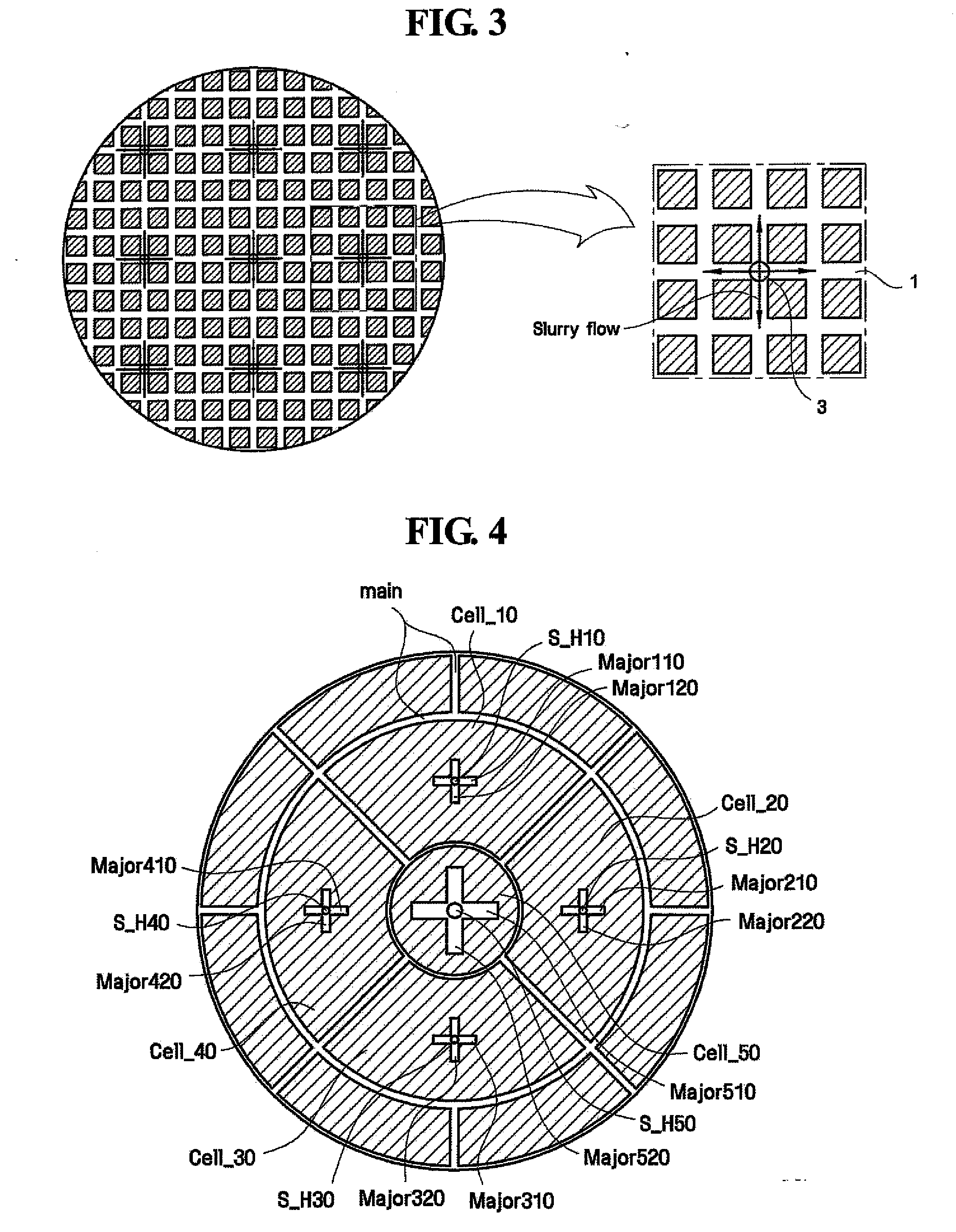
[0025] the polishing pad of the CMP apparatus according to the present invention will now be described with reference to FIG. 3.

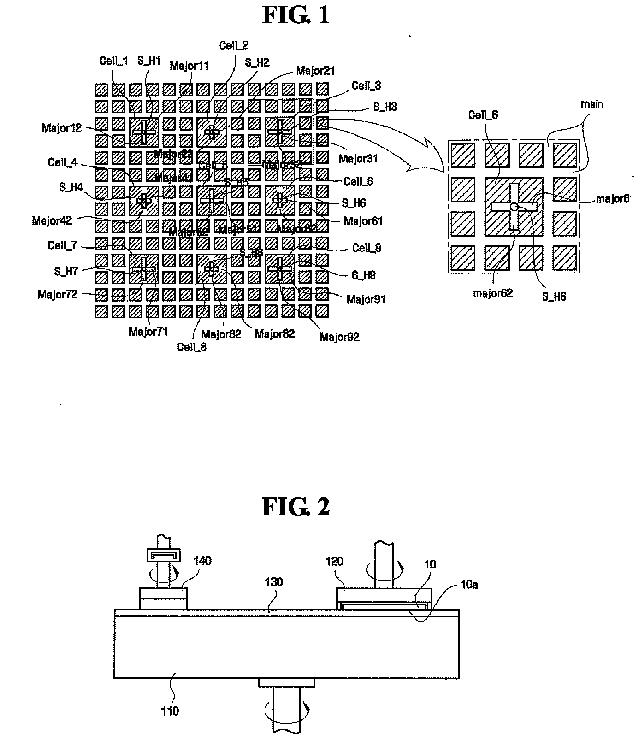
[0026] The polishing pad has an upper portion divided into a plurality of cells Cell_1 through Cell_9 by main grooves. The cells Cell_1 through Cell_9 are square and are delimited by the main grooves which are thus seen to extend along the periphery of the cells Cell_through Cell_9. The cells Cell_1 through Cell_9 consist of land portions, and grooved portions defined by first major grooves Major11 through Major91, respectively. In addition, a system slurry holes S_H1 through S_H9 extend through the body of the pad, and one or more slurry holes S_H1 through S_H9 are open to the first major grooves Major11 through Major91. Slurry for polishing the target surface of an object (e.g., a semiconductor substrate) is supplied to the slurry holes S_H1 through S_H9 via a passageway in the platen of the CMP apparatus (170 in FIG. 2).

[0027] The first major grooves Ma...

second embodiment

[0035] a polishing pad according to the present invention will now be described with reference to FIGS. 5 and 6.

[0036] The second embodiment of the polishing pad has a plurality of cells delimited by main grooves, and in this case, the grooved portion of a respective cell is defined by major and minor grooves. In addition, slurry holes extend through the body of the pad and are open to the major grooves within the cells, respectively. Even though this embodiment of the polishing pad may include nine cells arranged similarly to that shown in FIG. 3, only a sixth cell Cell_6 is illustrated in FIGS. 5 and 6 for the sake of simplicity. All of the cells have a structure similar to that of the sixth cell Cell_6 and therefore, only the structure of the polishing pad associated with this Cell_6 will be described in detail.

[0037] The cell Cell_6 is square. Main grooves extend within the upper surface of the pad to delimit the cell. Thus, main grooves are seen to extend along the periphery o...

third embodiment

[0043] a polishing pad of a CMP apparatus according to the present invention will now be described with reference to FIG. 7.

[0044] The third embodiment of the polishing pad has a plurality of cells, main grooves, and major and minor grooves extending within each of the cells. In addition, slurry holes extend through the body of the pad and are open to the upper surface of the pad within the cells, respectively. Even though this embodiment of the polishing pad may include nine cells arranged similarly to that shown in FIG. 3, only a sixth cell Cell_6 is illustrated in FIG. 7 for the sake of simplicity. All of the other cells have a structure similar to that of the sixth cell Cell_6 and therefore, only the structure of the polishing pad associated with this Cell_6 will be described in detail with reference to FIG. 7. Moreover, the third embodiment of the polishing pad is similar to that of the second embodiment of FIGS. 5 and 6 and thus, only that portion of the third embodiment which...


PUM


Abstract

A polishing pad for use in chemically mechanically polishing a semiconductor substrate enhances the uniformity of the rate at which material is removed from the surface of the semiconductor substrate, thereby ensuring the reproducibility of the chemical mechanical polishing process. The polishing pad has main grooves that divide an upper portion of the pad into a plurality of cells. At least one of the cells includes a land portion and a grooved portion substantially enclosed by the land portion. A respective slurry hole extends through the pad to the grooved portion such that slurry supplied through the slurry hole feeds into the grooved portion but is impeded by the land portion from flowing outwardly of the cell.

Description

CROSS-REFERENCE TO RELATED APPLICATIONS [0001] This is a divisional of application Ser. No. 11 / 169,731, filed Jun. 30, 2005, which is incorporated herein by reference in its entirety.BACKGROUND OF THE INVENTION [0002] 1. Field of the Invention [0003] The present invention relates to a chemical mechanical polishing (CMP) apparatus for polishing a semiconductor substrate. More specifically, the present invention relates to a polishing pad of the of the CMP apparatus. [0004] 2. Description of the Related Art[0005] Recently, the rapid development of data processing and communications technologies has led to the demand for semiconductor devices, such as Dynamic Random Access Memories (DRAMs), that operate rapidly and have large storage capacities. Accordingly, semiconductor device fabrication technology has been developed with the aim of enhancing the integration, reliability, and response speed of semiconductor devices. [0006] Fabricating semiconductor devices that have higher degrees o...

Claims


Application Information

Patent Timeline
Patent Type & Authority Applications(United States)
IPC IPC(8): B24B29/02B24B7/04B24D11/00
CPCB24B57/04B24B37/04Y02P70/10H01L21/304
Inventor PARK, MOO-YONGLEE, TAE-HOONKOO, JAE-EUNG
Owner SAMSUNG ELECTRONICS CO LTD
Why Eureka
Try Eureka