

MEMS device and fabrication method thereof
a technology of micro-electromagnetic system and mems device, which is applied in the direction of micro-structural technology, semiconductor devices, electrical apparatus, etc., can solve the problems of difficult to reduce the resistance value of the structure to the resistance value required, thinned structure may lose its mechanical strength, and direct affect the characteristics of the mems device, etc., to achieve stably silicidization, low resistance, and provide the effect of strength
- Summary
- Abstract
- Description
- Claims
- Application Information
AI Technical Summary
Benefits of technology
Problems solved by technology
Method used
Image

Examples
first embodiment
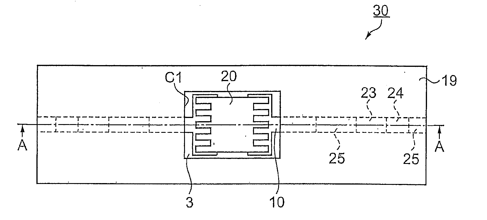
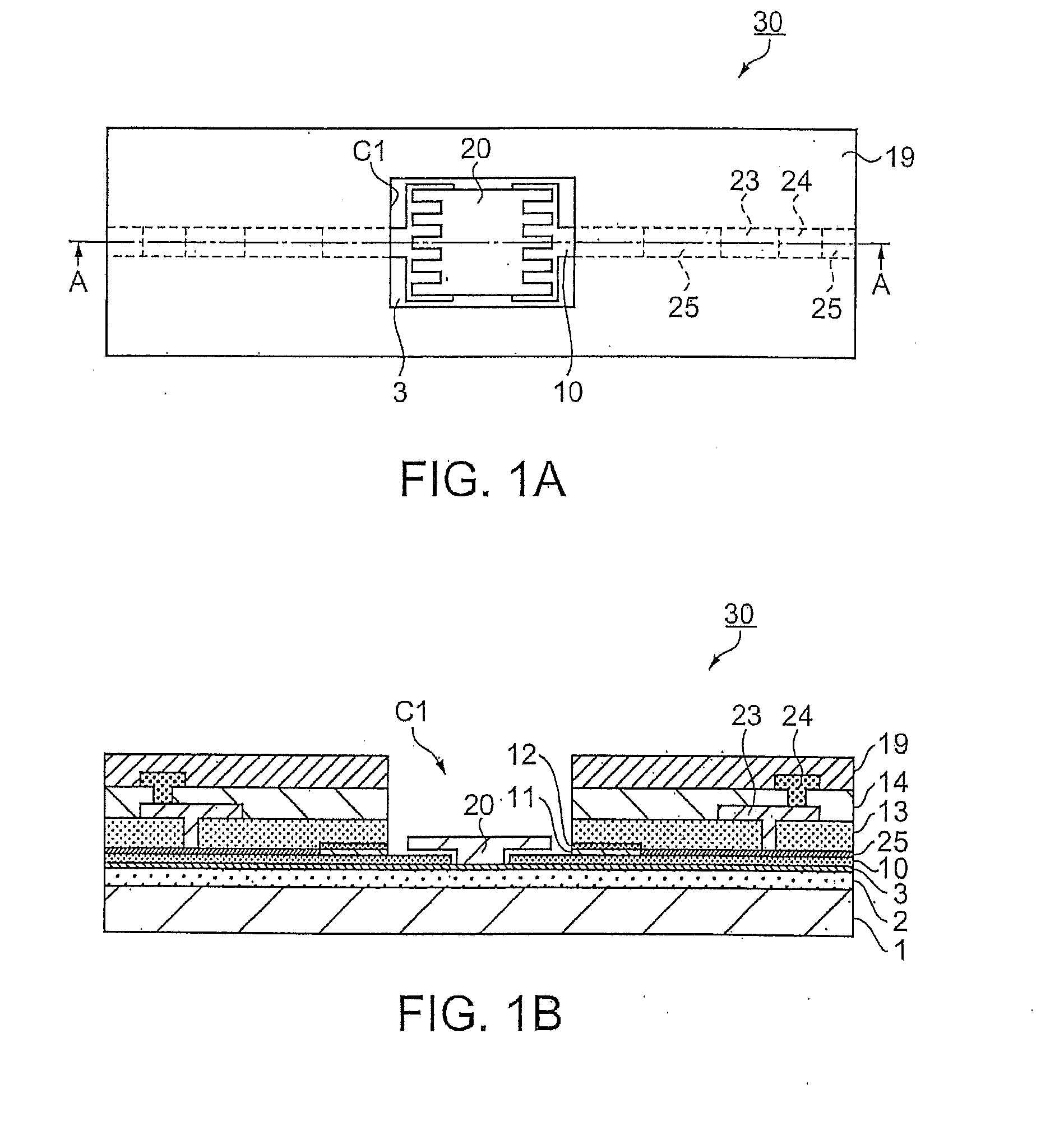
[0038]First, one example of a micro-electromechanical system (MEMS) device will be described in accordance with the drawings. FIG. 1A is a plan diagram showing a composition of the MEMS device of the first embodiment of the invention. FIG. 1B is a sectional diagram of FIG. 1A taken on a line A-A.
[0039]Referring to FIGS. 1A and 1B, a MEMS device 30 includes: a silicon substrate 1, a fixed electrode 10 fixed above the silicon substrate 1, and a wiring layered part that is layered above a portion of the fixed electrode 10 and composed of a first interlayer insulating film 13, a first wiring layer 23, a second interlayer insulating film 14, a second wiring layer 24, and a protection film 19. Also, a movable electrode 20 is provided in a movable state in an opening Cl formed in the approximate center of the wiring layered part. A silicide part 25 is provided at a portion of the fixed electrode 10 covered by the wiring layered part by silicidizing the surface of the portion.
[0040]Layered ...
second embodiment
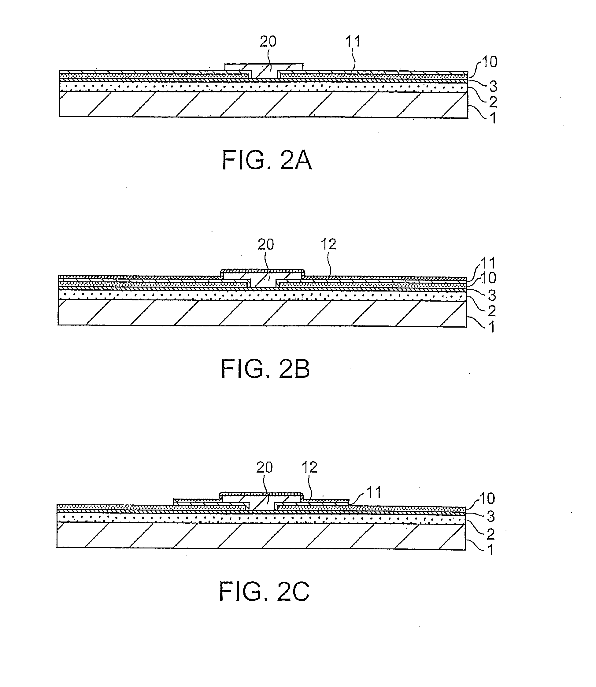
[0048]A method for fabricating the MEMS device 30 of the first embodiment will now be explained. FIGS. 2A to 2C, 3A to 3C, and 4A to 4D are schematic sectional diagrams explaining processes for fabricating the MEMS device 30. FIGS. 2A to 2C, 3A to 3C, and 4A to 4D show a section of the MEMS device 30 taken at the same position as in FIG. 1B.
[0049]To fabricate the MEMS device 30, semiconductor fabrication processes are used. Referring to FIG. 2A, the surface of the silicon substrate 1 is, for example, thermally oxidized to provide the insulating film 2 made of silicon oxide (SiO2). On the insulating film 2, the nitride film 3 composed of, for example, silicon nitride (SiN) is deposited by a process such as CVD or sputtering. This nitride film 3 becomes a base layer that will act as an etching stop layer used when conducting release etching as will be described hereafter.
[0050]Then, a polycrystalline silicon film is deposited by, for example, CVD on the nitride film 3 and, after being...
third embodiment
[0066]According to the MEMS device 30 of the first embodiment produced by the fabrication method of the second embodiment, the portion of the fixed electrode 10 that is unexposed to the release etchant when releasing the movable electrode 20 is silicidized to form the silicide part 25. In contrast, in the third embodiment, the silicide part is provided on a portion of the movable electrode and a portion of the fixed electrode that are exposed to the release etchant. The explanation thereof will follow with reference to a drawing.
[0067]FIG. 5 is a schematic sectional diagram to explain a MEMS device 70 of the third embodiment, the section thereof taken at the same position as in FIG. 1B in the first embodiment. The elements of the MEMS device 70 of the third embodiment that are identical to those of the MEMS device 30 are designated with the same reference numbers, and descriptions thereof will not be repeated.
[0068]With reference to FIG. 5, the MEMS device 70 includes: the silicon s...
PUM
 Abstract
Description
Claims
Application Information