Stack-type semiconductor package sockets and stack-type semiconductor package test systems

a technology of semiconductor package and test system, which is applied in the direction of individual semiconductor device testing, semiconductor/solid-state device details, instruments, etc., can solve the problems the limitation of reducing the size of the semiconductor package, and the inability to use the whole semiconductor packag

Active Publication Date: 2008-04-24
SAMSUNG ELECTRONICS CO LTD
View PDF3 Cites 26 Cited by
  • Summary
  • Abstract
  • Description
  • Claims
  • Application Information

AI Technical Summary

Problems solved by technology

However, since it is very difficult to reduce the size of the semiconductor chip, there is a limitation to reducing the size of the semiconductor package.
How ever, the multi-chip semiconductor package has a problem in that the whole semiconductor package can not be used when one of a plurality of semiconductor chips is defective or a wire for connecting the semiconductor chips is defective.
In this instance, it is not efficient that each package is inserted into each socket and the upper case is fixed.
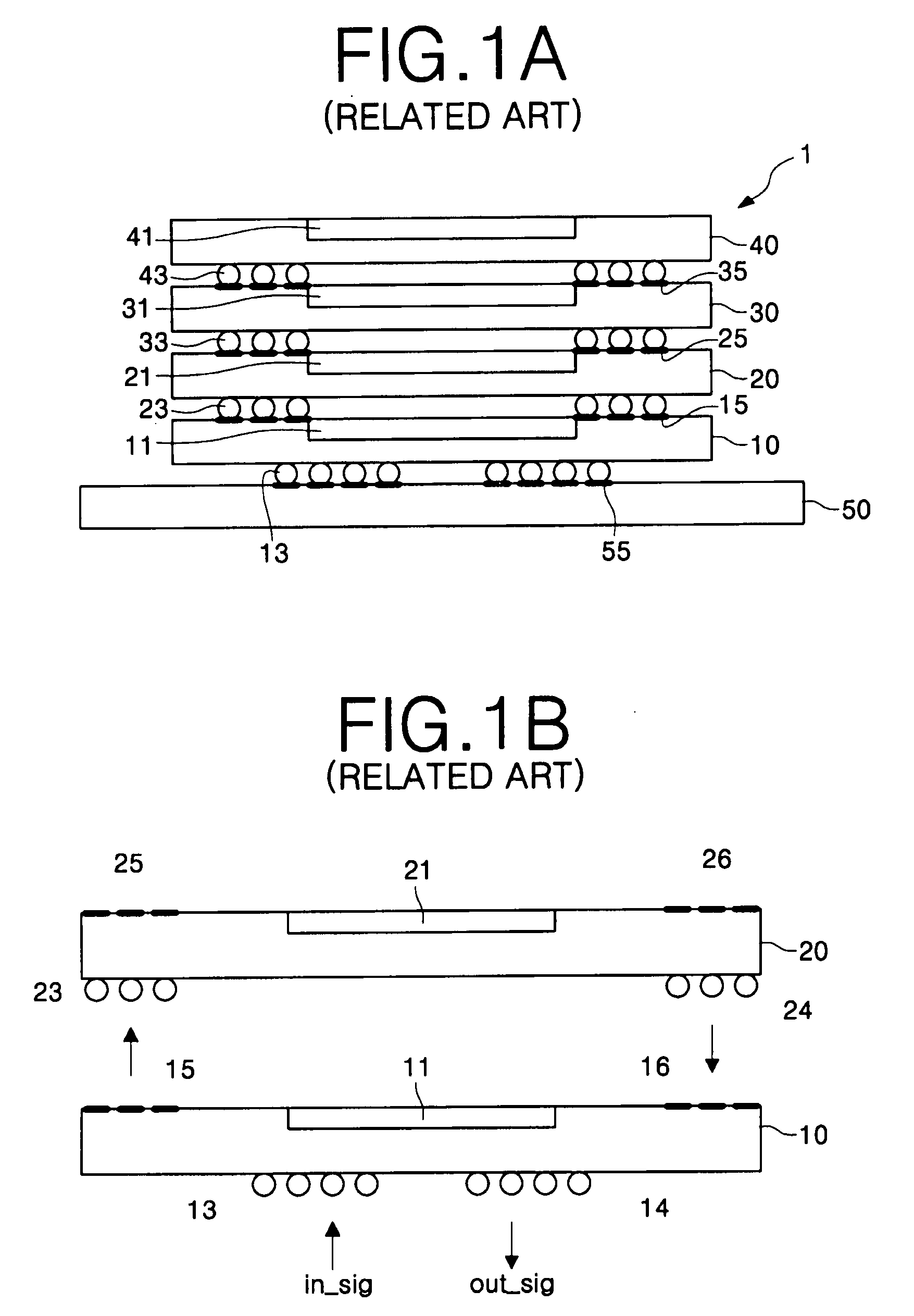
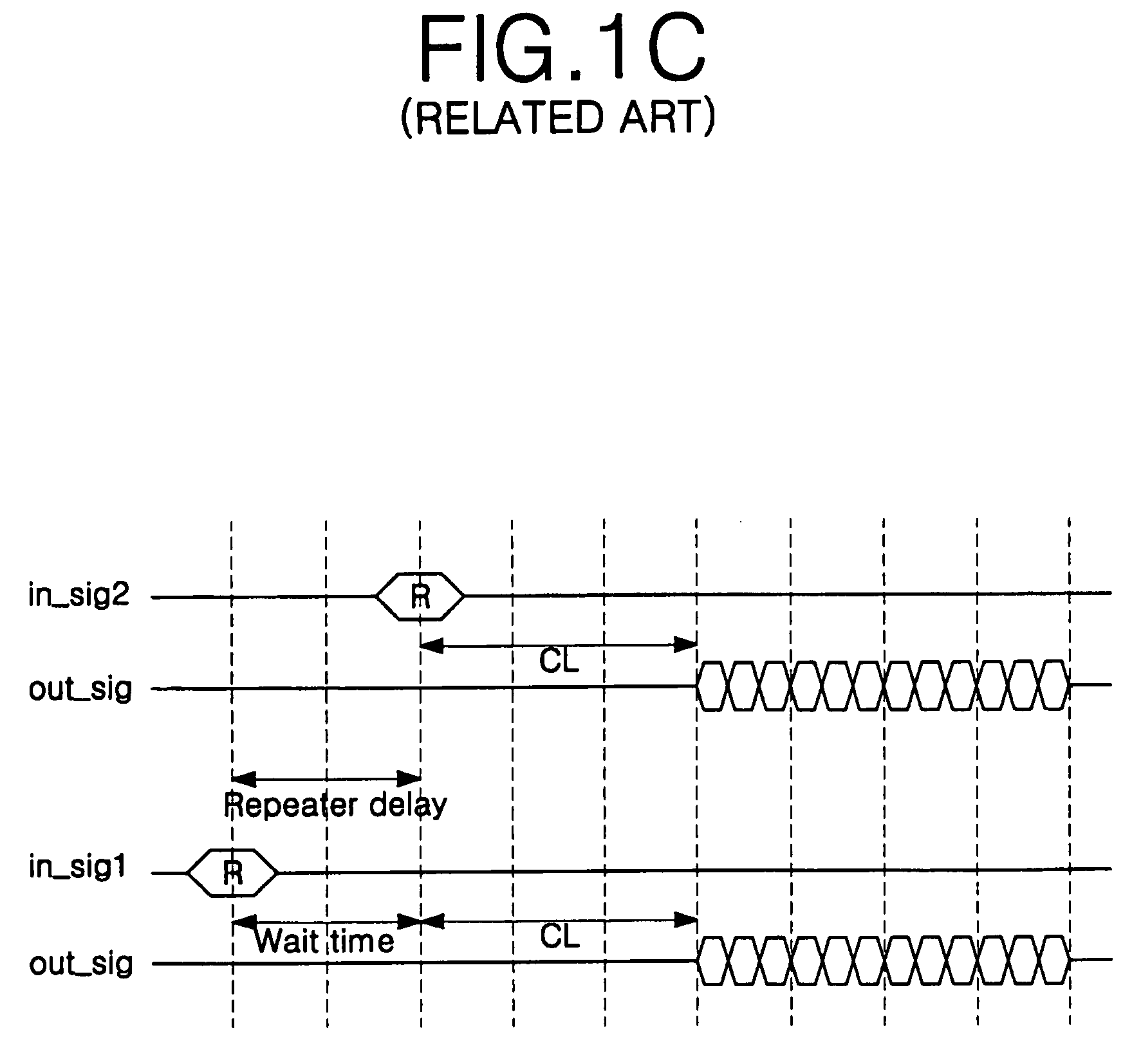
However, in case of the individual package test, a test for a function of the repeater is insufficient.
In case of the stack-type semiconductor package test, all functions including a function of the repeater can be tested, but when a defect occurs, the whole stack-type semiconductor package can not be used or the individual semiconductor packages stacked should be disassembled and reassembled, leading to an increment of repairing cost and time.
In addition, it is very difficult to find out which package has a problem in the stack-type semiconductor package.

Method used


Image

  • Stack-type semiconductor package sockets and stack-type semiconductor package test systems
  • Stack-type semiconductor package sockets and stack-type semiconductor package test systems
  • Stack-type semiconductor package sockets and stack-type semiconductor package test systems

Examples


Embodiment Construction

[0046]Example embodiments will now be described more fully with reference to the accompanying drawings. Embodiments, however, may be embodied in many different forms and should not be construed as being limited to the example embodiments set forth herein. Rather, these example embodiments are provided so that this disclosure will be thorough and complete, and will fully convey the scope to those skilled in the art. In the drawings, the thickness of layers and regions may be exaggerated for clarity.

[0047]It will be understood that when an element is referred to as being “on,”“connected to,”“electrically connected to,” or “coupled to” to another component, it may be directly on, connected to, electrically connected to, or coupled to the other component or intervening components may be present. In contrast, when a component is referred to as being “directly on,”“directly connected to,”“directly electrically connected to,” or “directly coupled to” another component, there are no interve...


PUM


Abstract

A stack-type semiconductor package socket may include: a first package connection portion for connection with leads of a lowermost package of a stack-type semiconductor package; a second package connection portion for connection between pads of an odd-numbered package and leads of an even-numbered package, wherein the odd-numbered package and the even-numbered package are adjacent to each other; a lower case for fixing the first package connection portion; and an upper case for fixing the second package connection portion. A stack-type semiconductor package test system may include: a stack-type semiconductor package socket that includes first and second package connection portions; a printed circuit board electrically connected to leads of the lowermost package through the first package connection portion; and a test controller for receiving, outputting, or receiving and outputting signals from, to, or from and to the stack-type semiconductor package through the PCB and the stack-type semiconductor package socket.

Description

PRIORITY STATEMENT[0001]This application claims priority from Korean Patent Application No. 10-2006-0103632, filed on Oct. 24, 2006, in the Korean Intellectual Property Office (KIPO), the entire contents of which are incorporated herein by reference.BACKGROUND[0002]1. Field[0003]Example embodiments relate to stack-type semiconductor packages. Also, example embodiments relate to stack-type semiconductor package sockets and / or stack-type semiconductor package test systems.[0004]2. Description of Related Art[0005]As a semiconductor manufacturing technology develops, a semiconductor package with higher integration has been realized. In addition, various electronic devices are pursuing multi-function and miniaturization, which means that the semiconductor packages should be made in smaller sizes while performing more functions.[0006]The size of the existing semiconductor packages greatly depends on the size of a semiconductor chip, and thus the size of the semiconductor package can be re...

Claims


Application Information

Patent Timeline
Patent Type & Authority Applications(United States)
IPC IPC(8): G01R31/02H01L23/48
CPCG01R1/0483G01R31/318505G01R31/31905H05K2201/10734H05K1/145H05K2201/045H05K1/141H01L2224/16225H01L2224/73253H01L23/12H01L23/02
Inventor KIM, WOO-SEOP
Owner SAMSUNG ELECTRONICS CO LTD
Why Eureka
Try Eureka