Multi-ground shielding semiconductor package, method of fabricating the package, and method of preventing noise using multi-ground shielding

Inactive Publication Date: 2008-05-01
SAMSUNG ELECTRONICS CO LTD
View PDF2 Cites 16 Cited by
  • Summary
  • Abstract
  • Description
  • Claims
  • Application Information

AI Technical Summary

Problems solved by technology

Thus, the propagated noise adversely affects the digital circuit block.
Even if the grounds of the analog and digital circuit blocks are isolated from each other though, high frequency noise of an analog signal may be propagated in the form of an electromagnetic wave.
Thus, the high frequency noise causes coupling between powers and grounds of the analog circuit blocks and those of the digital circuit blocks, and appears as noise in the digital circuit block.
A signal coupling problem occurs even in the conventional semiconductor package i

Method used


Image

  • Multi-ground shielding semiconductor package, method of fabricating the package, and method of preventing noise using multi-ground shielding
  • Multi-ground shielding semiconductor package, method of fabricating the package, and method of preventing noise using multi-ground shielding
  • Multi-ground shielding semiconductor package, method of fabricating the package, and method of preventing noise using multi-ground shielding

Examples


Embodiment Construction

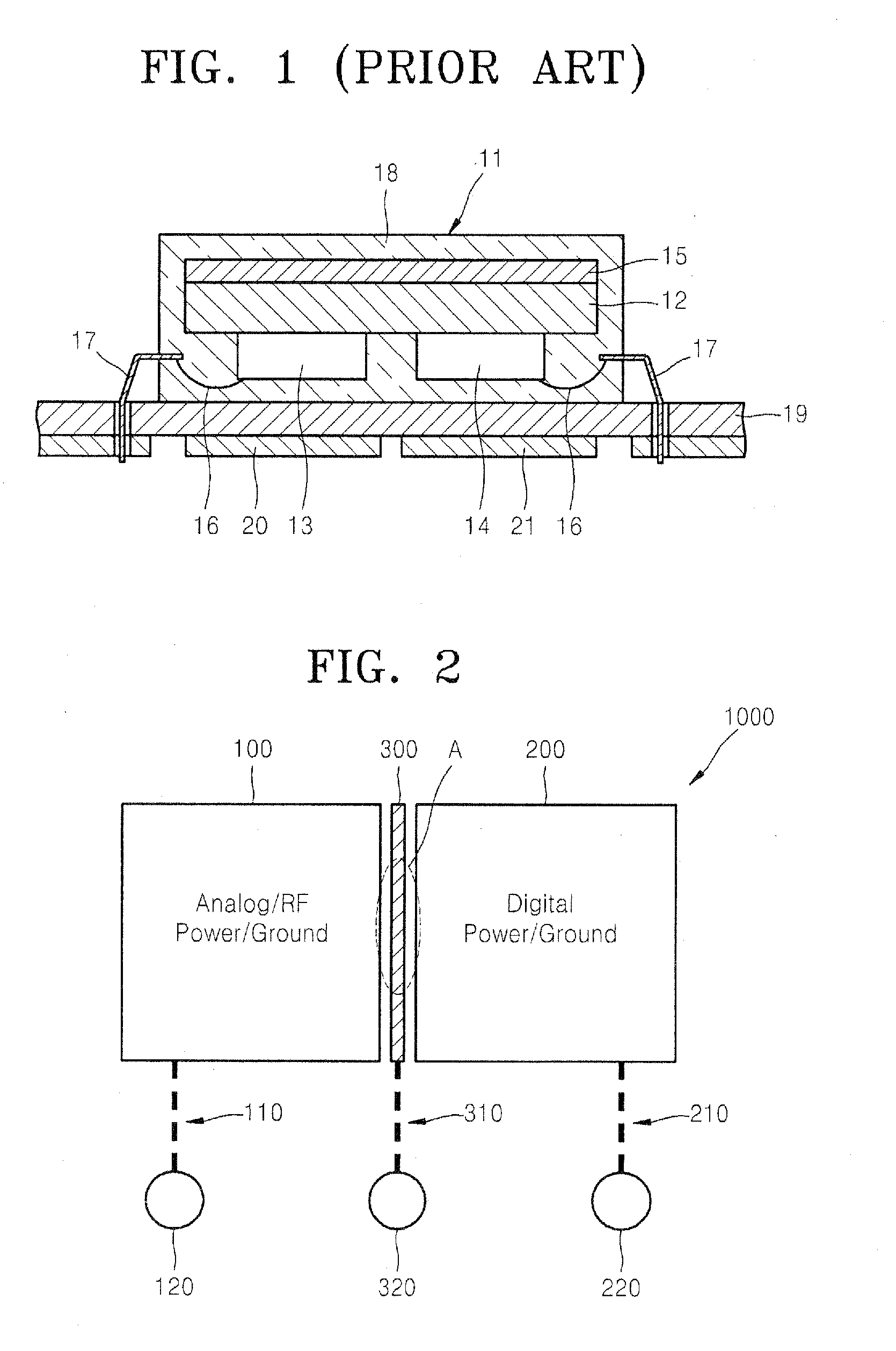
[0025]The invention will now be described more fully with reference to the accompanying drawings, in which exemplary embodiments of the invention are shown. The invention may, however, be embodied in many different forms and should not be construed as being limited to the embodiments set forth herein; rather, these embodiments are provided so that this disclosure will be thorough and complete, and will fully convey the concept of the invention to those skilled in the art. In the drawings, the thicknesses of layers and regions are exaggerated for clarity. It will also be understood that when a layer is referred to as being “on” another layer or substrate, it can be directly on the other layer or substrate, or intervening layers may also be present. Like reference numerals in the drawings denote like elements, and thus their description will be omitted.

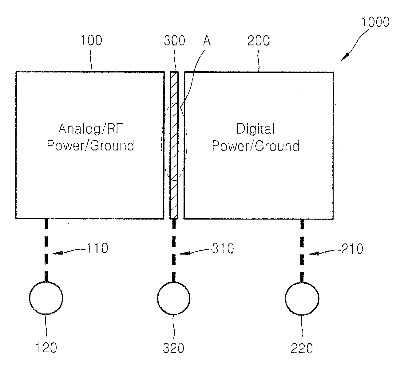
[0026]FIG. 2 is a plan view of a semiconductor package in which a ground shielding is formed between analog and digital circuit blocks...


PUM


Abstract

Provided are a multi-ground shielding semiconductor package including analog and digital circuit blocks and capable of preventing a coupling problem between the analog and digital circuit blocks caused by high frequency noise. A method of fabricating the multi-ground shielding semiconductor package, and a method of preventing noise in the multi-ground shielding semiconductor package are also provided. The multi-ground shielding semiconductor package includes at least one semiconductor chip; and a circuit board on which the semiconductor chip is mounted and on which a plurality of circuit blocks are formed, wherein a conductive ground shielding is formed between the circuit blocks and separately from grounds of the circuit blocks to prevent noise between the circuit blocks.

Description

CROSS-REFERENCE TO RELATED PATENT APPLICATION[0001]This application claims the benefit of Korean Patent Application No. 10-2006-0105550, filed on Oct. 30, 2006, in the Korean Intellectual Property Office, the disclosure of which is incorporated herein by reference in its entirety.BACKGROUND[0002]1. Technical Field[0003]The invention relates to a semiconductor device and a method of fabricating the same, and more particularly, to a semiconductor package including analog and digital circuit blocks, a method of fabricating the semiconductor package, and a method of preventing noise in the semiconductor package.[0004]2. Description of the Related Art[0005]Aided by the high integration of semiconductor devices, semiconductor packages in which analog and digital circuit blocks are integrated have become popular in recent times. For example, a plurality of circuit blocks are formed in a semiconductor package such as a package including analog / digital mixed signal chips, a system in package...

Claims


Application Information

Patent Timeline
IPC IPC(8): H01L39/00
CPCH01L23/552H01L23/66H01L2924/3025H01L2924/30107H01L2924/01322H01L2224/48247H01L2224/48091H01L2223/6688H01L2924/00014H01L2924/00H01L2924/181H01L2224/023H01L2924/00012H01L2924/0001H01L23/60H01L23/58
Inventor SONG, EUN-SEOKLEE, HEE-SEOK
Owner SAMSUNG ELECTRONICS CO LTD
Why Eureka
Try Eureka