Wafer stacked package having vertical heat emission path and method of fabricating the same

a technology of stacked packages and heat emission paths, which is applied in the direction of semiconductor devices, semiconductor/solid-state device details, electrical apparatus, etc., can solve the problems of large ineffective dissipation of heat in the middle of the stack, and ‘hot spot phenomenon’, so as to reduce the amount of heat generated, improve the thermal reliability of the wsp, and reduce the effect of heat buildup

Active Publication Date: 2008-05-01
SAMSUNG ELECTRONICS CO LTD
View PDF4 Cites 47 Cited by
  • Summary
  • Abstract
  • Description
  • Claims
  • Application Information

AI Technical Summary

Benefits of technology

[0015]The vertical heat emission path reduces the heat buildup in the WSP due to the heat generated by the semiconductor chips and quickly dissipates a large amount of heat during the operation of the WSP. Consequently, the thermal reliability of the WSP is improved.

Problems solved by technology

This can cause a ‘hot spot’ phenomenon when the NAND flash device operates at high speed.
When a stack is formed of four or more chips with a relatively high power consumption, such as high-speed DDR DRAMs, a large amount of heat is generated.
In a WSP particularly, the heat in the middle of the stack can not be effectively dissipated, since a significant amount of an adhesive is used for bonding the stack.
This reduces the reliability of the WSP.
The vertical heat emission path reduces the heat buildup in the WSP due to the heat generated by the semiconductor chips and quickly dissipates a large amount of heat during the operation of the WSP.

Method used


Image

  • Wafer stacked package having vertical heat emission path and method of fabricating the same
  • Wafer stacked package having vertical heat emission path and method of fabricating the same
  • Wafer stacked package having vertical heat emission path and method of fabricating the same

Examples


Embodiment Construction

[0034]The present invention will now be described more fully with reference to the accompanying drawings, in which preferred embodiments of the invention are shown. This invention may, however, be embodied in many different forms, and should not be construed as being limited to the embodiments set forth herein. Rather, these embodiments are provided so that this disclosure will be thorough and complete, and will fully convey the scope of the invention to those skilled in the art.

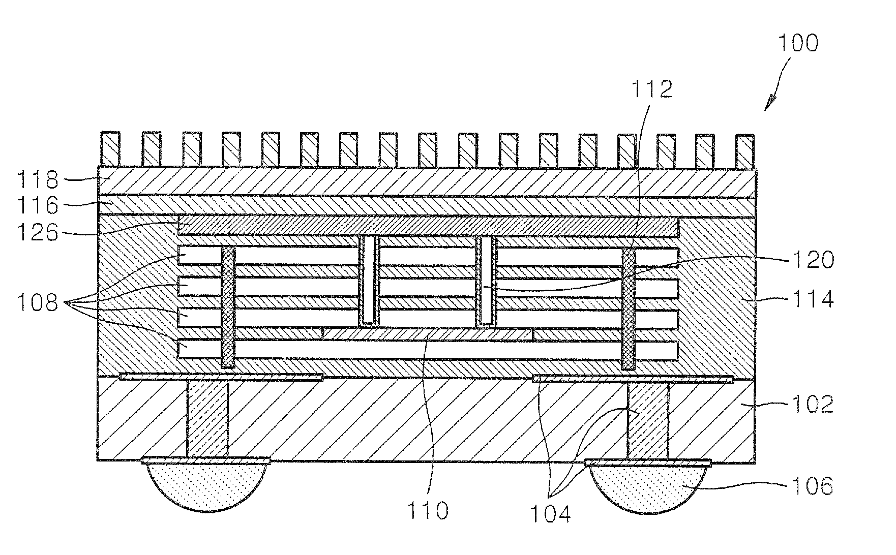
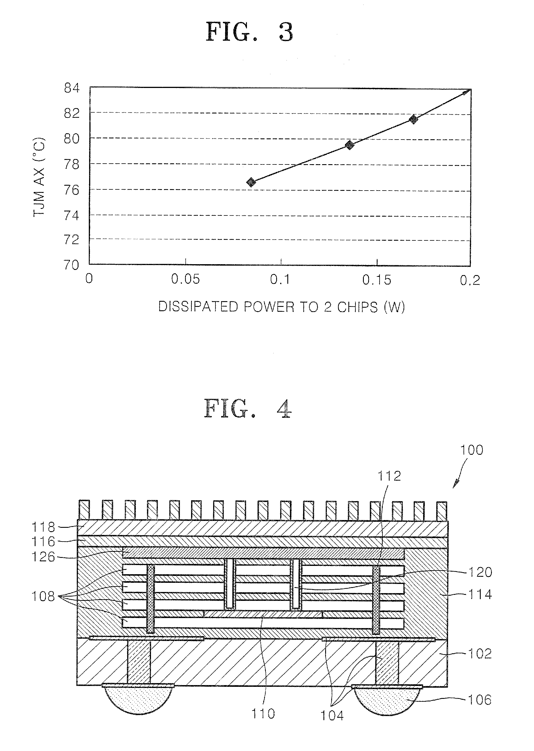
[0035]FIG. 4 is a sectional view of a wafer stacked semiconductor package (WSP) having a vertical heat emission path, according to an embodiment of the present invention.

[0036]As illustrated in FIG. 4, the WSP 100 comprises: a substrate 102 on which a printed circuit pattern 104 is formed, a plurality of semiconductor chips 108 mounted vertically on the substrate 102, a cooling through-hole 120 formed vertically through the plurality of semiconductor chips 108 and sealed, a micro hole (122 of FIG. 7) formed ...


PUM


Abstract

A wafer stacked semiconductor package (WSP) having a vertical heat emission path and a method of fabricating the same are provided. The WSP comprises a substrate on which semiconductor chips are mounted; a plurality of semiconductor chips stacked vertically on the substrate; a cooling through-hole formed vertically in the plurality of semiconductor chips, and sealed; micro holes formed on the circumference of the cooling through-hole; and a coolant filling the inside of the cooling through-hole. Accordingly, the WSP reduces a temperature difference between the semiconductor chips and quickly dissipates the heat generated by the stacked semiconductor chips.

Description

CROSS-REFERENCE TO RELATED PATENT APPLICATION[0001]This application claims priority under 35 USC § 119 to Korean Patent Application No. 10-2006-0105628, filed on Oct. 30, 2006 in the Korean Intellectual Property Office, the disclosure of which is incorporated herein in its entirety by reference.BACKGROUND[0002]1. Technical Field[0003]The present invention relates to a semiconductor package and a method of fabricating the same, and more particularly, to a wafer stacked package (WSP) having a vertical heat emission path inside a WSP semiconductor chip, and a method of fabricating the same.[0004]2. Description of the Related Art[0005]Conventionally, the usual method of fabricating a semiconductor memory device with high integration density is to apply the design rules of fabricating a thinner wafer and positioning many integrated circuits within the small area of the wafer, so that elements such as transistors and capacitors are three-dimensionally arranged. As an alternative, semicond...

Claims


Application Information

Patent Timeline
Patent Type & Authority Applications(United States)
IPC IPC(8): H01L23/34H01L21/58
CPCH01L23/427H01L23/481H01L24/90H01L25/0657H01L2224/73253H01L2225/06541H01L2224/9202H01L2924/14H01L2924/15311H01L24/24H01L24/82H01L2224/24145H01L2225/06589H01L23/34H01L23/36
Inventor BAEK, JOONG-HYUNLEE, HEE-JIN
Owner SAMSUNG ELECTRONICS CO LTD
Why Eureka
Try Eureka