Image forming apparatus
a technology of image forming apparatus and transfer current, which is applied in the direction of electrographic process apparatus, instruments, optics, etc., can solve the problems of difficult to avoid the interference phenomenon of the image forming apparatus, lack of transfer current to generate defective images, etc., and achieve the effect of reducing image defects and reducing image defects
- Summary
- Abstract
- Description
- Claims
- Application Information
AI Technical Summary
Benefits of technology
Problems solved by technology
Method used
Image
Examples
first embodiment
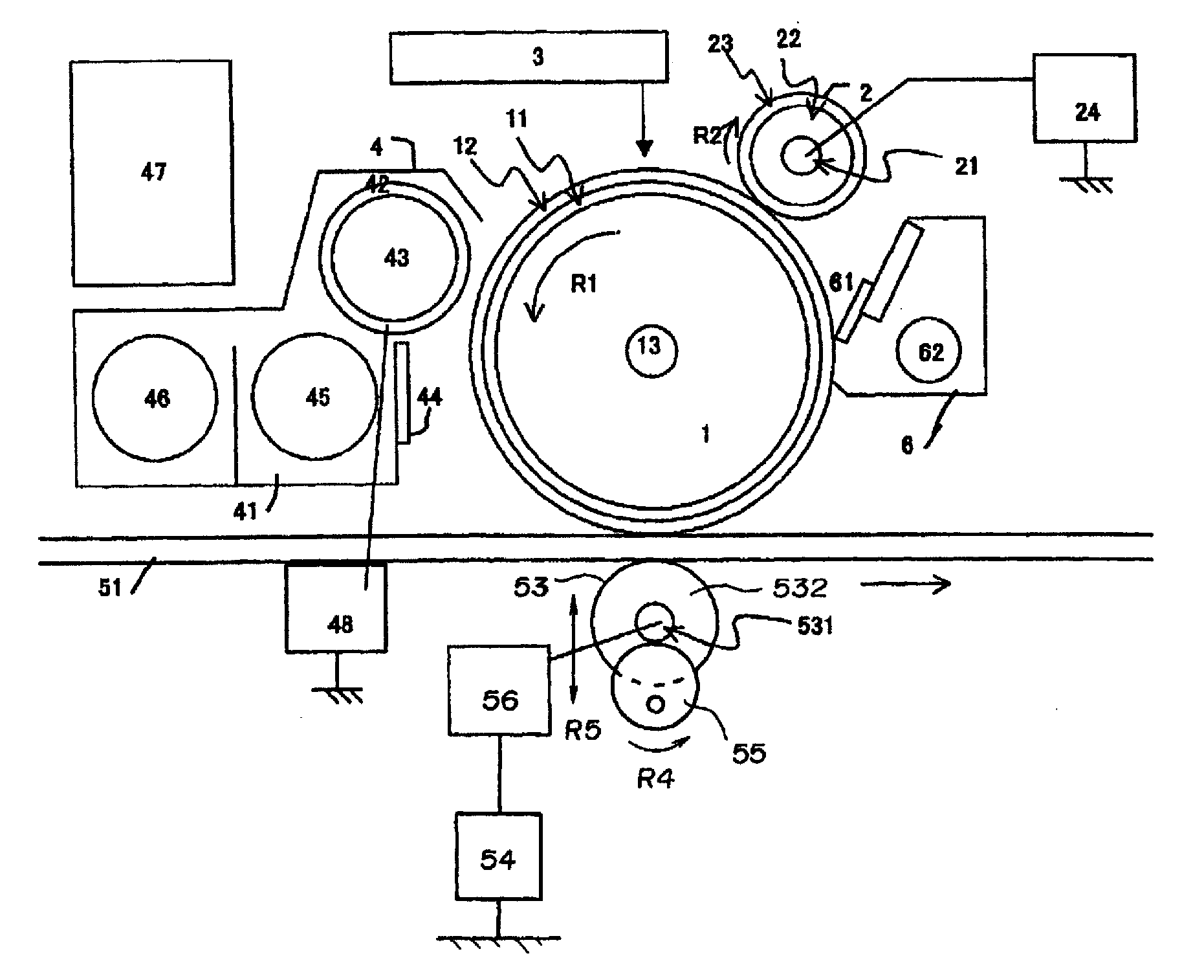
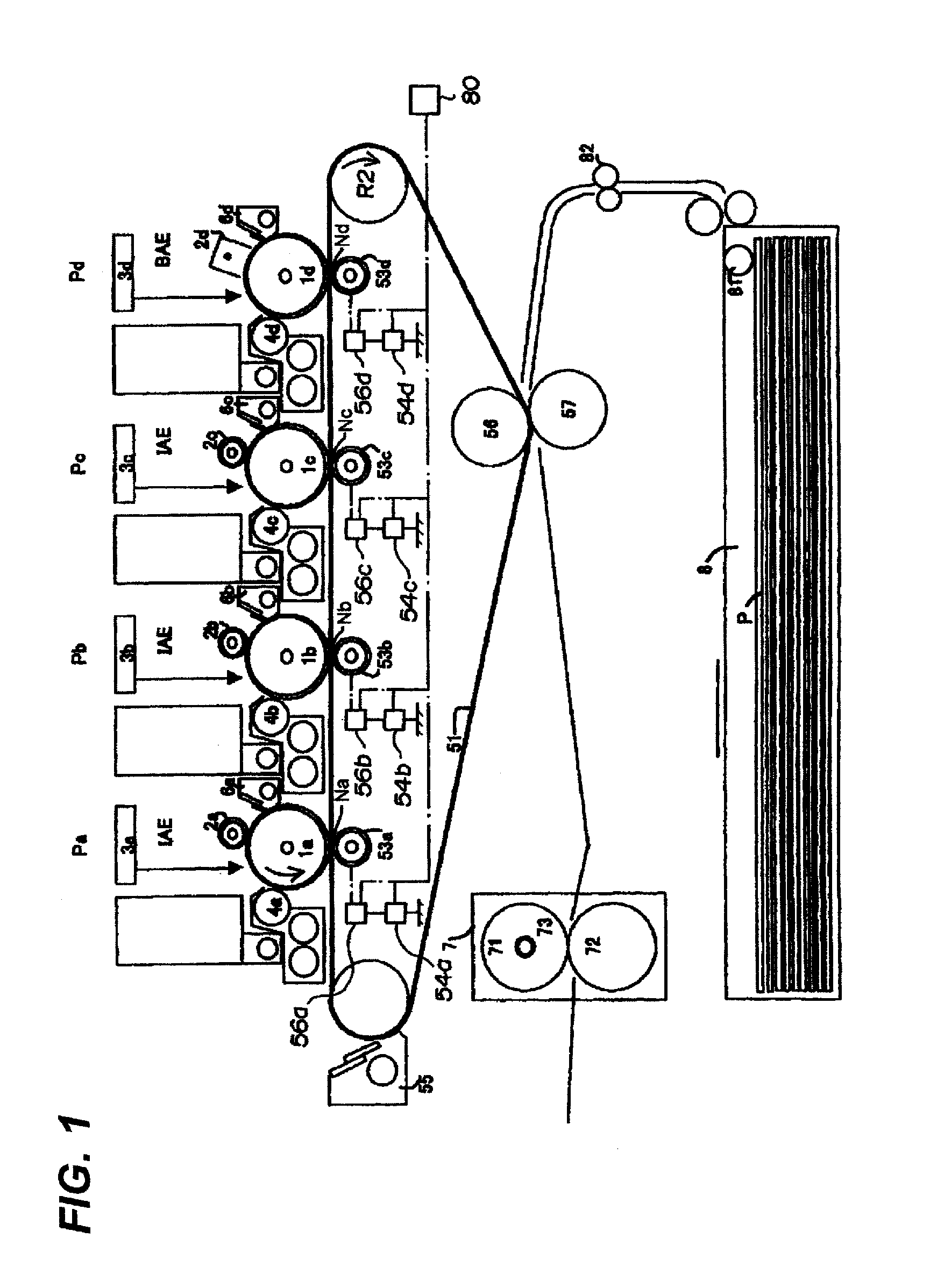
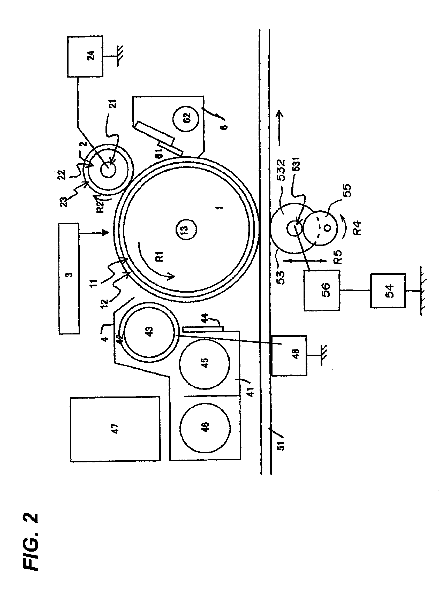
[0040]FIG. 1 shows a schematic configuration of an image forming apparatus according to a first embodiment of the invention. The image forming apparatus of the first embodiment includes four image forming portions. The image forming apparatus is a full-color electrophotographic image forming apparatus, in which toner images formed in the image forming portions are primary-transferred to an intermediate transfer member and the primary-transferred image is secondary-transferred to a recording medium to obtain a color image.
[Overall Configuration of Image Forming Apparatus]
[0041]An overall configuration of the image forming apparatus will be described. As shown in FIG. 1, process units Pa, Pb, Pc, and Pd which are of the four image forming portions are horizontally arranged to form the images of yellow Y, magenta M, cyan C, and black K colors. Photosensitive drums 1a, 1b, 1c, and 1d are arranged in the process units Pa, Pb, Pc, and Pd while being able to be rotated in an arrow directio...
second embodiment
[0083]A second embodiment of the invention is based on a transfer bias control method in the case where a lower-resistance intermediate transfer belt is used. A configuration and an operation of an image forming apparatus of the second embodiment are similar to those of the first embodiment, so that only the configuration and control different from the first embodiment will be described in detail.
[0084]In the second embodiment, a PI resin having the surface resistivity of 1011Ω / □ (with a probe conformable to JIS-K6911, at applied voltage of 100 V for applied time of 60 sec, at 23° C. and 50% RH) and the thickness t of 100 μm is used as the intermediate transfer belt 51. The intermediate transfer belt 51 is formed by an ion-conductive belt member, and the intermediate transfer belt 51 has the advantages such as low cost and low unevenness of resistance. At the same time, a resistance fluctuates largely depending on environmental temperature and humidity, and the resistance is decreas...
third embodiment
[0091]A third embodiment of the invention is based on an apparatus in which control for setting an optimum transfer bias, called ATVC, is used in the transfer bias application is performed by the constant-voltage control. A configuration and an operation of an image forming apparatus of the third embodiment are similar to those of the first embodiment, so that only the configuration and control different from the first embodiment will be described in detail.
[0092]In the transfer roller, not only a variation in resistance is hardly suppressed during production, but also the resistance is changed by environmental temperature and humidity changes or deterioration. In ATVC, the transfer voltage is detected when the desired transfer current is passed through the transfer roller 53 at timing except for the usual image formation, and the detected transfer voltage is applied at constant during the image formation.
[0093]The third embodiment is based on the transfer bias control method for av...
PUM
 Abstract
Description
Claims
Application Information


