

Solder ball mounting method and solder ball mounting substrate manufacturing method
- Summary
- Abstract
- Description
- Claims
- Application Information
AI Technical Summary
Benefits of technology
Problems solved by technology
Method used
Image

Examples
Embodiment Construction
[0044]Next, exemplary embodiments for carrying out the present invention will be explained with reference to the drawings hereinafter.
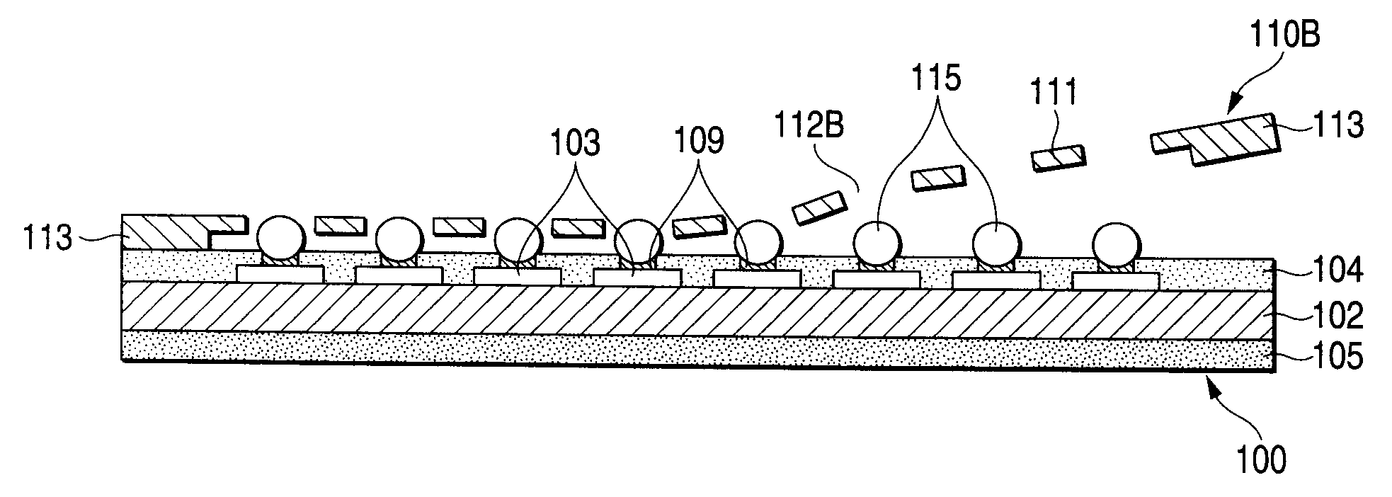
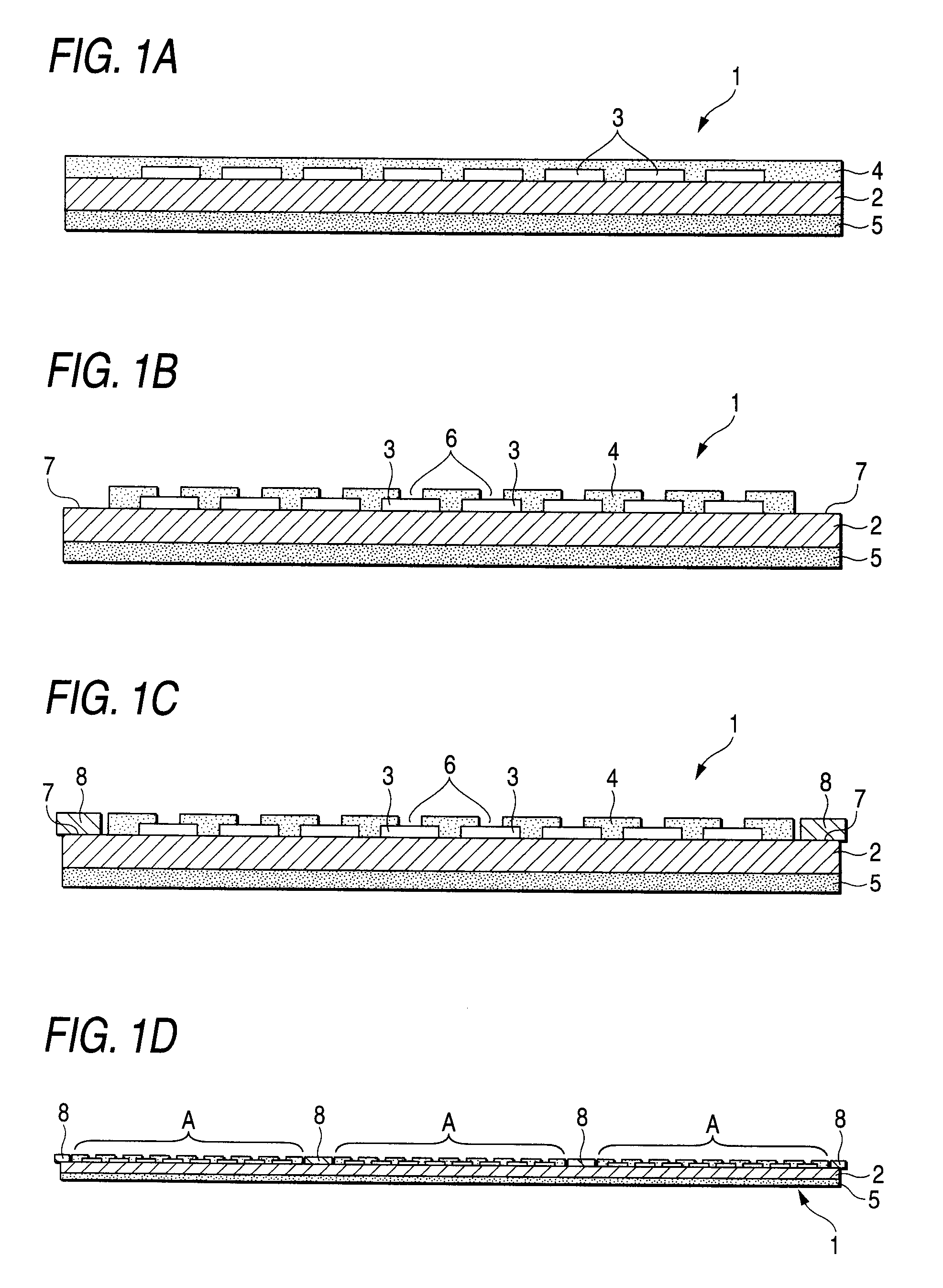
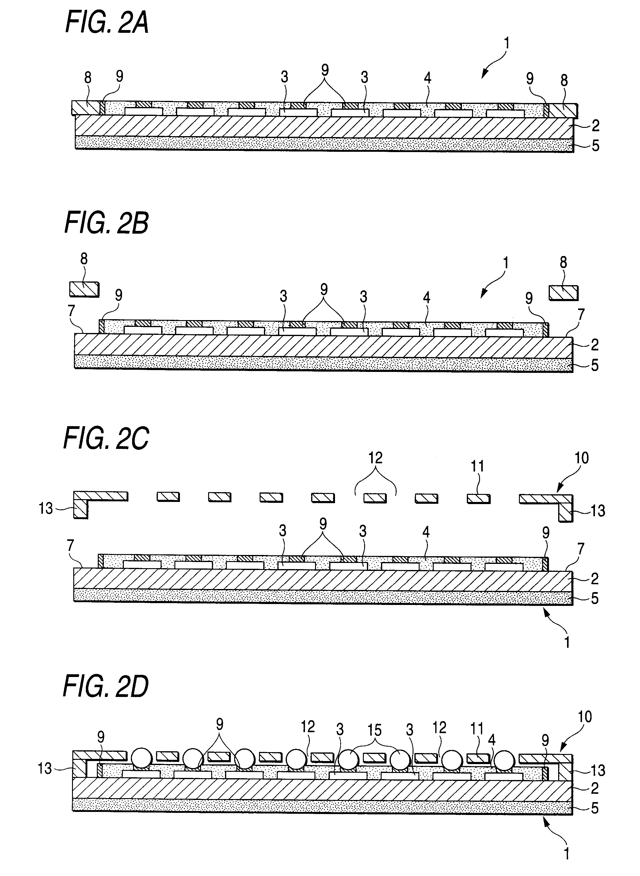
[0045]FIG. 1A to FIG. 3D are views explaining a solder ball mounting method as an embodiment of the present invention in line with process procedures. FIG. 1A shows a substrate 1. This substrate 1 is constructed by a substrate main body 2, a solder resist 4 formed on an upper surface of the substrate main body 2, and an insulating film 5 formed on a lower surface of the substrate main body 2.
[0046]As the substrate main body 2, various types of substrates such as a resin substrate, a ceramic substrate, an Si wafer, a build-up substrate, and the like can be applied. A plurality of electrodes 3 are formed on the upper surface of the substrate main body 2.
[0047]In the present embodiment, assume that an example where a wafer is used as the substrate main body 2 will be explained hereunder. Also, a large number of element areas are formed on the wafer. In F...
PUM
 Abstract
Description
Claims
Application Information