Object exchange method, exposure method, carrier system, exposure apparatus, and device manufacturing method

a technology of carrier system and exposure method, which is applied in the direction of photomechanical equipment, instruments, printers, etc., can solve the problems of high probability of throughput decrement, weaker intensity of 450 mm wafer compared to 300 mm wafer, and difficulty in putting it into practi

Active Publication Date: 2010-11-25
NIKON CORP
View PDF48 Cites 125 Cited by
  • Summary
  • Abstract
  • Description
  • Claims
  • Application Information

AI Technical Summary

Benefits of technology

[0023]According to this apparatus, it is not necessary to form a notch in the holding member to house an arm and the like used for unloading to unload ...

Problems solved by technology

However, because the thickness of the wafer does not increase in proportion to the size of the wafer, intensity of the 450 mm wafer is much weaker when compared to the 300 mm wafer.
Accordingly, even when addressing an issue such as wafer carriage, is expected that putting it into practice would be difficult in the same ways and means as in the current 300 mm wafer.
Further, when the size of the wafer becomes as large as 450 mm, while the number of dies (chips) output from a single wafer increases, the probability becomes high o...

Method used


Image

  • Object exchange method, exposure method, carrier system, exposure apparatus, and device manufacturing method
  • Object exchange method, exposure method, carrier system, exposure apparatus, and device manufacturing method
  • Object exchange method, exposure method, carrier system, exposure apparatus, and device manufacturing method

Examples


first embodiment

A First Embodiment

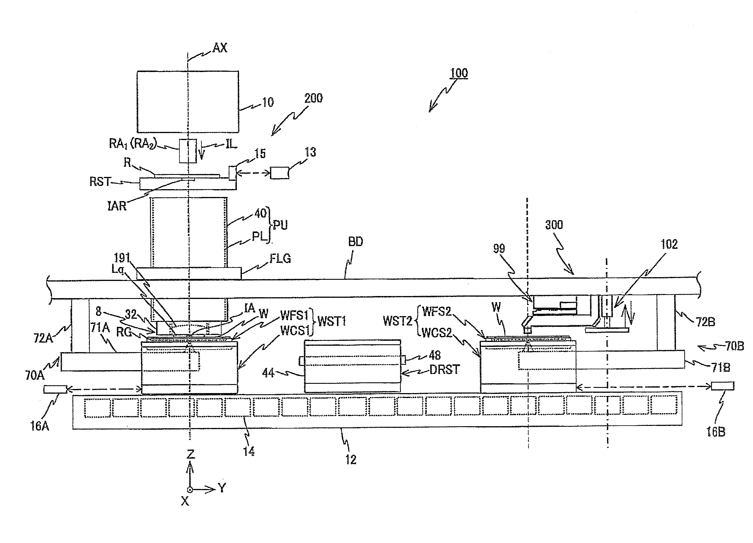
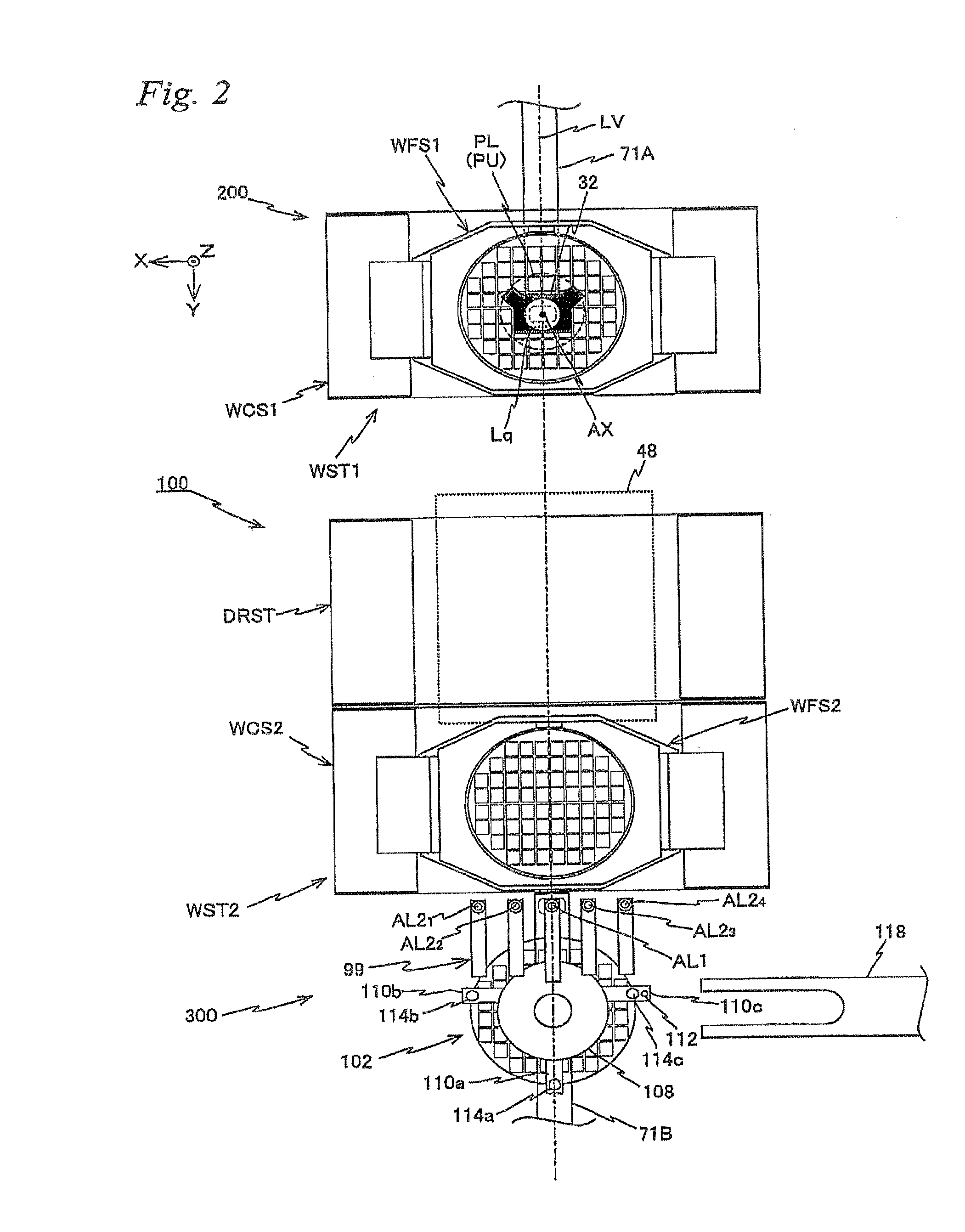
[0100]A first embodiment of the present invention will be described below, with reference to FIGS. 1 to 22C.

[0101]FIG. 1 schematically shows a configuration of an exposure apparatus 100 in the first embodiment. Exposure apparatus 100 is a projection exposure apparatus by the step-and-scan method, or a so-called scanner. As it will be described later, a projection optical system PL is arranged in the embodiment, and in the description below, a direction parallel to an optical axis AX of this projection optical system PL will be described as the Z-axis direction, a direction within a plane orthogonal to the Z-axis direction in which a reticle and a wafer are relatively scanned will be described as the Y-axis direction, a direction orthogonal to the Z-axis direction and the Y-axis direction will be described as the X-axis direction, and rotational (inclination) directions around the X-axis, the Y-axis, and the Z-axis will be described as θ x, θ y, and θ z directions, ...

second embodiment

A Second Embodiment

[0264]Hereinafter, a second embodiment of the present invention will be described, with reference to FIGS. 25 to 41C. Here, from a viewpoint of avoiding repetition, the same or similar reference numerals will be used for the same or similar sections as in the first embodiment previously described, and a detailed description thereabout will be simplified or omitted.

[0265]FIG. 25 shows a schematic configuration of an exposure apparatus 1000 in the second embodiment when viewed from the +X side, and FIG. 26 shows a partially omitted planar view of exposure apparatus 1000. Further, FIG. 27 shows a center table and the vicinity of a chuck unit which will be described later on. Further, FIG. 28A shows a side view of a wafer stage which exposure apparatus 1000 is equipped with when viewed from the −Y direction, and FIG. 28B shows a planar view of the wafer stage, respectively. FIG. 29A is a planar view of a coarse movement stage, FIG. 29B is a planar view showing a state...

third embodiment

A Third Embodiment

[0314]A third embodiment of the present invention will be described below, with reference to FIGS. 42 to 59. Here, from a viewpoint of avoiding repetition, the same or similar reference numerals will be used for the same or similar sections as in the first and second embodiments previously described, and a detailed description thereabout will be simplified or omitted.

[0315]FIG. 42 shows a schematic configuration of an exposure apparatus 2000 in the third embodiment in a planar view. Exposure apparatus 2000 is a projection exposure apparatus by the step-and-scan method, or a so-called scanner.

[0316]As shown in FIG. 42, exposure apparatus 2000 is equipped with an exposure station 200 in which exposure to wafer W is performed, a measurement station 300 placed away by a predetermined distance to the +Y side of exposure station 200, a center table 130 placed between measurement station 300 and exposure station 200, two wafer stages WST1 and WST2, an unload table 150 pla...


PUM


Abstract

A carrier apparatus positions a chuck member above a wafer mounted on a fine movement stage, relatively moves the chuck member and the fine movement stage in a vertical direction, makes the chuck member approach a position which is a predetermined distance away from the upper surface of the wafer, makes the chuck member hold the wafer from above in a non-contact manner, and makes the chuck member holding the wafer and the fine movement stage move apart within a predetermined plane after making the chuck member holding the wafer and the fine movement stage move apart in the vertical direction. Further, the carrier apparatus loads the wafer held in a non-contact manner from above by the chuck member on the fine movement stage.

Description

CROSS-REFERENCE TO RELATED APPLICATIONS[0001]This non-provisional application claims the benefit of Provisional Application No. 61 / 179,914 filed May 20, 2009, Provisional Application No. 61 / 213,329 filed May 29, 2009, and Provisional Application No. 61 / 213,330 filed May 29, 2009, the disclosures of which are hereby incorporated herein by reference in its entirety.BACKGROUND OF THE INVENTION[0002]1. Field of the Invention[0003]The present invention relates to object exchange methods, exposure methods, carrier systems, exposure apparatuses, and device manufacturing methods, and more particularly, to an exchange method in which a thin plate-shaped object is exchanged on a holding member, an exposure method using the exchange method, a carrier system which carries a thin plate-shaped object, an exposure apparatus which is equipped with the carrier system, and a device manufacturing method which uses the exposure method or the exposure apparatus.[0004]2. Description of the Background Art...

Claims


Application Information

Patent Timeline
IPC IPC(8): G03F7/20G03B27/52B65G1/133
CPCG03F7/70691G03F7/707G03F7/70733H01L21/6838H01L21/67225H01L21/67748G03F7/70775
Inventor SHIBAZAKI, YUICHI
Owner NIKON CORP
Why Eureka
Try Eureka