

IC tag and method for fabricating the same
- Summary
- Abstract
- Description
- Claims
- Application Information
AI Technical Summary
Benefits of technology
Problems solved by technology
Method used
Image

Examples
first embodiment
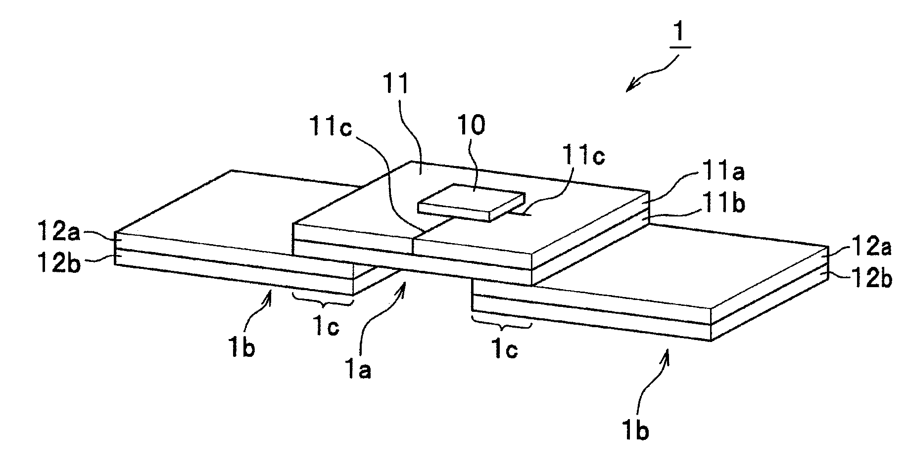
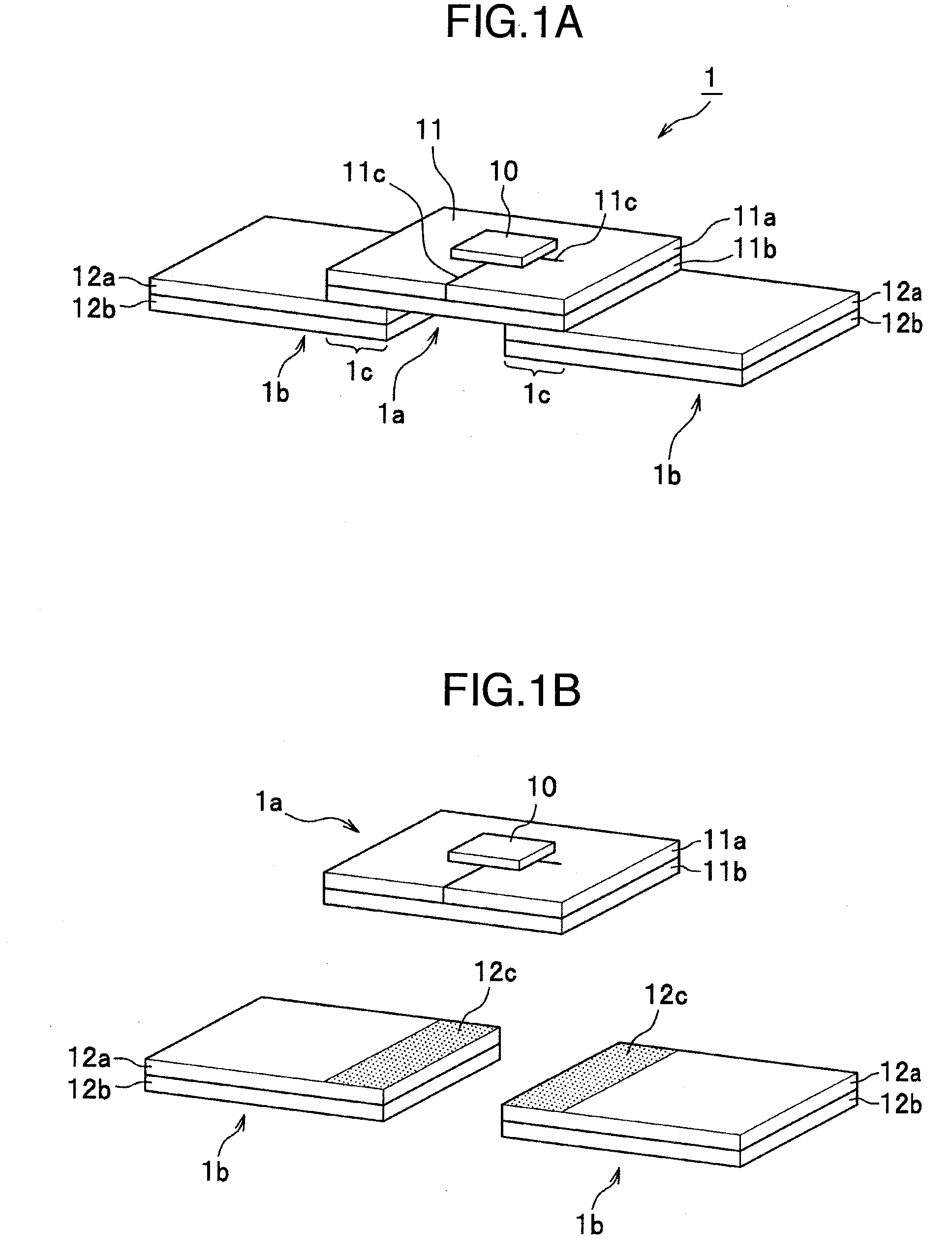
[0029]FIGS. 1A and 1B show an RFID tag as a first embodiment of this invention, FIG. 1A showing the RFID tag in its assembled state and FIG. 1B showing the same in its disassembled state.
[0030]As shown in FIGS. 1A and 1B, the REID tag (IC tag) 1 as the first embodiment of this invention is composed of an inlet 1a consisting of an antenna (first antenna) 11 as the main antenna and an IC chip 10 mounted thereon, and two conductor pieces (second antennas) 1b, 1b as the auxiliary antennas.
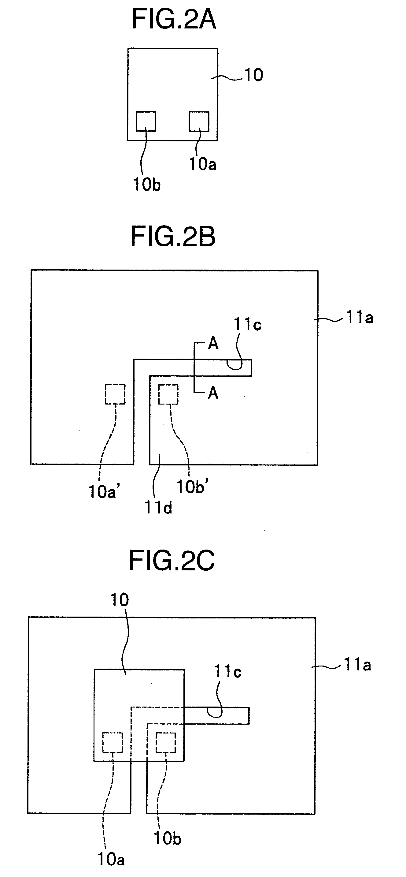
[0031]The antenna 11 is a metal film layer 11a of Au or Al having a thickness of several micrometers (μm), formed on a roughly rectangular base 11b of insulating material such as PET (polyethylene terephthalate) resin or PEN (polyethylene naphthalate) resin by vapor deposition using sputtering. The metal film layer 11a is provided with a slit 11c. The formation of the metal film layer 11a is not limited to the use of vapor deposition. For example, it may be formed with Au or Al metal paste printed on a...
second embodiment
[0052]FIGS. 4A, 4B and 4C show the structure of an RFID tag as a second embodiment of this invention. FIG. 4A shows a belt-like base with a metal film layer formed thereon; FIG. 4B shows an RFID tag as a second embodiment of this invention, which is built by folding the belt-like base; and FIG. 4C shows a variation of the second embodiment shown in FIG. 4B.
[0053]As shown in FIG. 4A, in the second embodiment of this invention, two metal film layers (second antennas) 20b, 20b of Au or Al having a thickness of several micrometers (μm) are formed on the belt-like base 20 of insulating material such as PET resin or PEN resin, separated from each other along the lengthwise direction the belt-like base 20, by vapor deposition using sputtering. Further, a metal film layer 20a is formed between the separated metal film layers 20b, 20b by using the same technique. The formation of the metal film layers 20a and 20b, 20b are not limited to the use of vapor deposition. They may be formed, for ex...
third embodiment
[0067]FIGS. 5A, 5B and 5C show the structure of an RFID tag as a third embodiment of this invention. FIG. 5A is the side view of the RFID tag as the third embodiment of this invention, FIG. 5B is the top view of the RFID tag as the third embodiment of this invention, and FIG. 5C is the bottom view of thr RFID tag as the third embodiment of this invention.
[0068]As shown in FIG. 5B, in the third embodiment of this invention, a metal film layer 30a of Au or Al having a thickness of several micrometers (μm) is formed on one surface (hereafter referred to as top or obverse surface) S of a belt-like base 30 of insulating material such as PET resin or PEN resin by vapor deposition using sputtering. Then, as shown in FIG. 5C, two metal film layers 30b, 30b of Au or Al having a thickness of several micrometers (μm) are formed on the other surface (hereafter referred to as bottom or reverse surface) R of the belt-like base 20, separated from each other along the lengthwise direction of the be...
PUM
 Abstract
Description
Claims
Application Information