Hybrid flash memory device and method for assigning reserved blocks thereof

a hybrid flash memory and reserved block technology, applied in memory adressing/allocation/relocation, digital storage, instruments, etc., can solve the problems of multi-bit arrays having a higher possibility of invalid sensing, data stored on volatile semiconductor devices is lost, and eproms have difficulty in rewriting stored data

Active Publication Date: 2008-05-15
SAMSUNG ELECTRONICS CO LTD
View PDF4 Cites 181 Cited by
  • Summary
  • Abstract
  • Description
  • Claims
  • Application Information

AI Technical Summary

Problems solved by technology

Data stored on a volatile semiconductor device is lost if a power supply is interrupted, while a non-volatile memory device retains stored data even when the power supply is interrupted.
The MROMs, PROMs, and EPROMs have difficulty in rewriting stored data because read and write operations cannot be freely conducte

Method used


Image

  • Hybrid flash memory device and method for assigning reserved blocks thereof
  • Hybrid flash memory device and method for assigning reserved blocks thereof
  • Hybrid flash memory device and method for assigning reserved blocks thereof

Examples


Embodiment Construction

[0019]The present invention will now be described more fully hereinafter with reference to the accompanying drawings, in which exemplary preferred embodiments of the invention are shown. This invention, however, may be embodied in many different forms and should not be construed as limited to embodiments set forth herein. Rather, embodiments are provided so that this disclosure will be thorough and complete, and will fully convey the scope of the invention to those skilled in the art. Like numbers refer to like elements throughout.

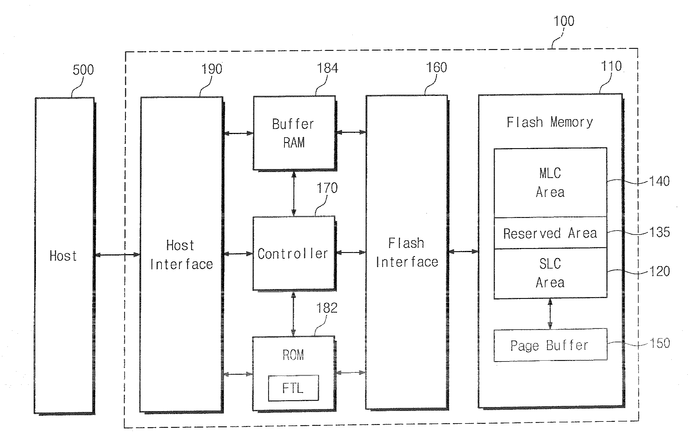
[0020]FIG. 1 illustrates a configuration of a hybrid flash memory device 100 according to an embodiment of the present invention. Specifically, the hybrid flash memory device 100 is a hybrid OneNAND flash memory device in which at least two memory cells differing in the number of stored bits per cell are formed on the same chip.

[0021]Referring to FIG. 1, the hybrid flash memory device 100 interfaces with a host 500 through a host interface 190. The host in...


PUM


Abstract

A hybrid flash memory device includes an array including a first area and a second area having a larger number of stored bits per cell than the first area The device includes a hidden area including a first reserved block area and a second reserved block area, wherein the first reserved block area includes a plurality of first memory blocks having the same number of stored bits per cell as the first area, the second reserved block area includes a plurality of second memory blocks having the same number of stored bits per cell as the second area, and a flash translation layer configured to replace a bad block generated in the first main area with the first memory block and replace a bad block generated in the second main area with the second memory block, wherein the flash translation layer flexibly assigns functions of the first memory blocks or the second memory blocks depending on whether the first and second memory blocks are all used.

Description

CROSS-REFERENCE TO RELATED APPLICATIONS[0001]This U.S. non-provisional patent application claims priority under 35 U.S.C §119 of Korean Patent Application 2006-104151 filed on Oct. 25, 2006, the entirety of which is hereby incorporated by reference.BACKGROUND[0002]1. Technical Field[0003]The present invention relates to semiconductor memory devices and, more specifically, to a method for assigning reserved blocks of a hybrid flash memory device in which single-bit cells and multi-bit cells are arranged in the same array.[0004]2. Description of Related Art[0005]Semiconductor memory devices may be categorized as volatile memory devices or non-volatile memory devices. The volatile memory devices can be classified into dynamic random access memories (DRAMs) and static random access memories (SRAMs). Data stored on a volatile semiconductor device is lost if a power supply is interrupted, while a non-volatile memory device retains stored data even when the power supply is interrupted. Thu...

Claims


Application Information

Patent Timeline
IPC IPC(8): G11C29/00G11C16/04G11C11/34G11C7/00
CPCG11C11/5621G11C2211/5641G11C29/82G11C16/0408G06F12/02G06F12/00
Inventor KIM, SEON-TAEKLEE, BYOUNG-KOOK
Owner SAMSUNG ELECTRONICS CO LTD
Why Eureka
Try Eureka