Printed circuit board and method for manufacturing thereof

Inactive Publication Date: 2008-05-29
SAMSUNG ELECTRO MECHANICS CO LTD
View PDF4 Cites 7 Cited by
  • Summary
  • Abstract
  • Description
  • Claims
  • Application Information

AI Technical Summary

Benefits of technology

[0009]An aspect of the present invention is to provide a printed circuit board (PCB) with high efficiency of heat dissipation and a method for manufacturing the printed circuit board by delivering the heat held in an insulating layer to a heat dissipating layer by forming a heat dissipating coating layer with high thermal conductivity on a heat dissipating layer.

Problems solved by technology

However, as the number of passive elements and packages mounted in the PCB is increased, so also are the amount of power consumption and the amount of heat generated, whereby the efficiency of heat dissipation is becoming an important decision criterion in terms of reliability and consumer preferences.
However, since the Prepreg, the electrical Conductive Adhesive, and the insulating resin are made of polymer materials, there is difficulty in effectively transferring heat to the heat dissipating layer.
Consequently, there is a problem of low efficiency in heat dissipation.

Method used


Image

  • Printed circuit board and method for manufacturing thereof
  • Printed circuit board and method for manufacturing thereof
  • Printed circuit board and method for manufacturing thereof

Examples


Embodiment Construction

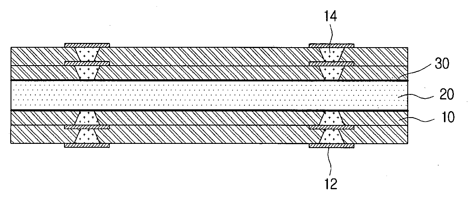
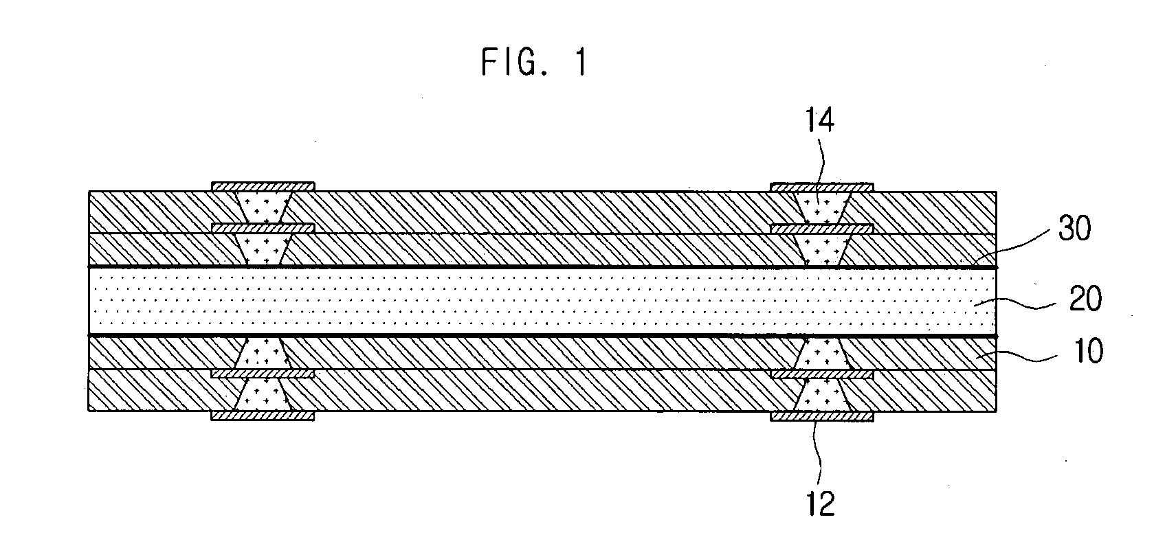
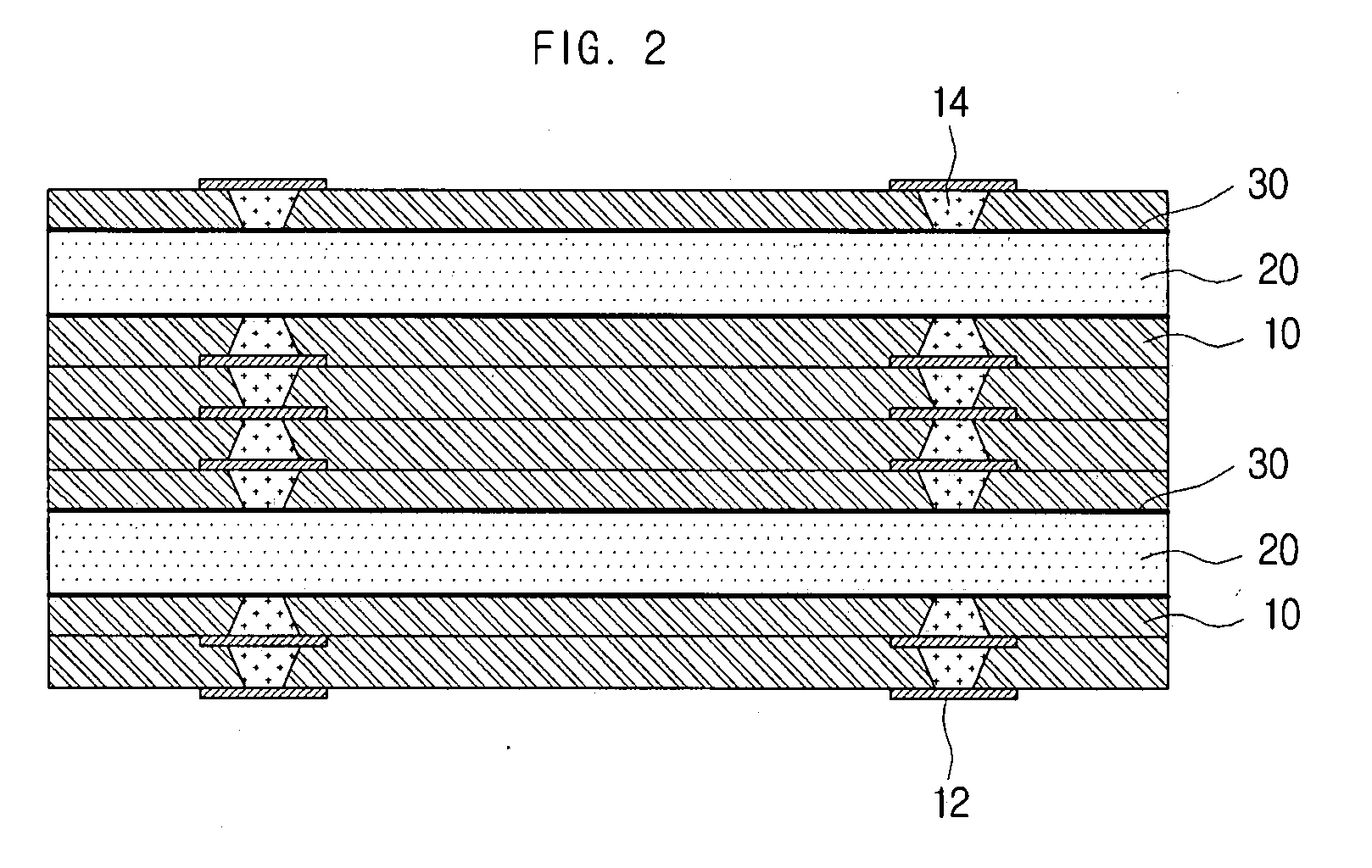
[0026]Embodiments of the printed circuit board according to the invention will be described below in more detail with reference to the accompanying drawings. In the description with reference to the accompanying drawings, those components are rendered the same reference number that are the same or are in correspondence, regardless of the figure number, and redundant explanations are omitted.

[0027]FIG. 1 is a cross-sectional view showing a printed circuit board according to an embodiment of the present invention, and FIG. 2 is a cross-sectional view showing a printed circuit board according to a second disclosed embodiment of the present invention. Referring to FIGS. 1 and 2, insulating layers 10, circuit patterns 12, bumps 14, a heat dissipating layer 20 and heat dissipating coating layers 30 are illustrated.

[0028]The insulating layers 10 may be made of Prepreg (PPG). The circuit patterns 12 and the bumps 14 may be formed in the insulating layer 10.

[0029]While Prepreg is presented a...


PUM

PropertyMeasurementUnit
Electrical conductoraaaaaaaaaa
Heataaaaaaaaaa

Abstract

A printed circuit board and a method of manufacturing thereof are disclosed. With a printed circuit board comprising an insulating layer; a circuit pattern formed on one side of the insulating layer; an inter-layer conductive part joining with the insulating layer by passing through the insulating layer, and electrically connected to the circuit pattern; a heat dissipating layer laminated on the other side of the insulating layer; and a heat dissipating coating layer interposed between the insulating layer and the heat dissipating layer, and connected with the inter-layer conductive part, the heat contained in the insulating layer may be delivered to the heat dissipating layer effectively and the efficiency of heat dissipation may be improved.

Description

CROSS-REFERENCE TO RELATED APPLICATIONS[0001]This application claims the benefit of Korean Patent Application No. 10-2006-0055844 filed with the Korean Intellectual Property Office on Jun. 21, 2006, the disclosure of which is incorporated herein by reference in its entirety.BACKGROUND[0002]1. Technical Field[0003]The present invention relates to a printed circuit board and a method for manufacturing thereof.[0004]2. Description of the Related Art[0005]Presently, as electronic products are becoming thinner and given more functionalities, a greater number of passive elements and higher density and multi layer packages are being mounted in a printed circuit board (PCB). This trend is expected to continue in the future. On a basic level, the printed circuit board has performed the role of connecting various kinds of electronic elements or supporting components according to the design of circuit patterns. However, as the number of passive elements and packages mounted in the PCB is incre...

Claims


Application Information

Patent Timeline
IPC IPC(8): H05K1/05H05K3/10
CPCH05K1/0206H05K1/0207H05K1/056H05K3/4069H05K3/4614Y10T29/49155H05K3/4647H05K3/4652H05K2201/0323H05K2201/096H05K2203/1189H05K3/4641H05K2201/0191H05K1/02H05K7/20
Inventor LEE, EUNG-SUEKYANG, DEK-GINKIM, KEUN-HO
Owner SAMSUNG ELECTRO MECHANICS CO LTD
Why Eureka
Try Eureka