Light emitting device

a technology of light-emitting devices and light-emitting elements, which is applied in the direction of semiconductor devices, semiconductor/solid-state device details, electrical devices, etc., can solve the problems of color mixing of light, increased brightness of light-emitting elements, and reduced color mixing, so as to achieve the minimum non-uniform color balance and improve color mixing.

Inactive Publication Date: 2008-06-05
NICHIA CORP
View PDF8 Cites 38 Cited by
  • Summary
  • Abstract
  • Description
  • Claims
  • Application Information

AI Technical Summary

Benefits of technology

[0007]The present invention is an object thereof to provide a high-quality light emitting device which can be improving color mixing and kept to a minimum nonuniform of color balance.
[0009]With the present invention, a high-quality light emitting device is obtained with which two light emitting element can be mounted on different members, and the distance between them is kept to a minimum, so that even under harsh environments such as use for extended periods, the requirement for higher drive speed and brighter light emitting elements can be satisfied while also preventing a disturbance of color balance and improving color mixing.

Problems solved by technology

With a light emitting device such as this, however, the lead frames have to be kept apart so they do not touch each other, so the elements have to be disposed away from each other, and this is a problem in that color mixing of the light suffers.
However, when a light source featuring light emitting elements such as these is driven under harsher conditions, such as when the drive speed is raised, the brightness of the light emitting elements is increased, or the device is used for extended periods, the heat generated by the driving of the light emitting elements themselves shifts the wavelength of the light emitted from the light emitting elements.
In particular, when light emitting elements that generate a large enough quantity of heat to become a heat source and light emitting elements whose wavelength fluctuates over a wide range are mounted in contact on the same substrate and / or on the same layer, color becomes unbalanced as the temperature rises.
This loss of color balance leads to a critically adverse effect due to minute fluctuations in characteristics, as in optical printer devices and scanners that sense by using electrical and optical characteristics.

Method used


Image

  • Light emitting device
  • Light emitting device
  • Light emitting device

Examples


example 1

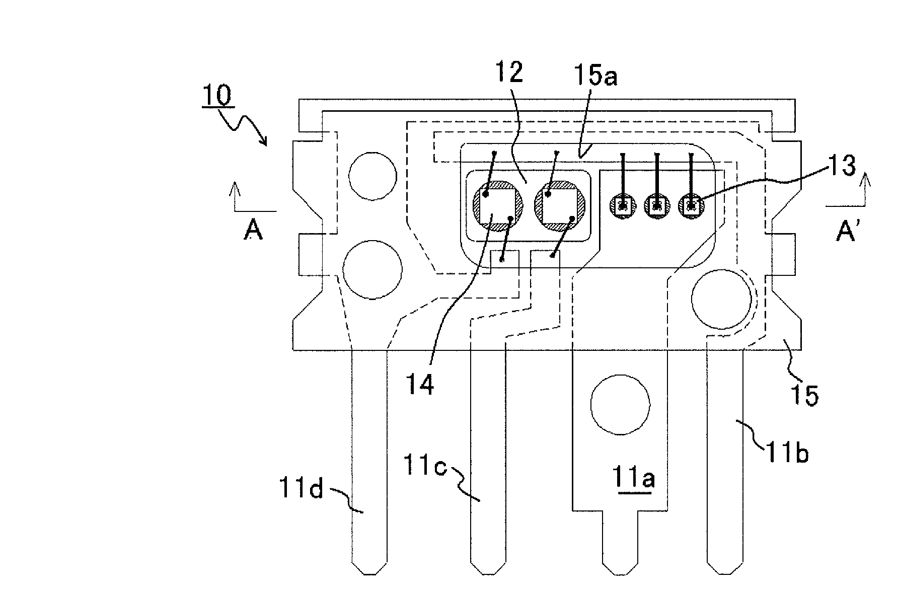
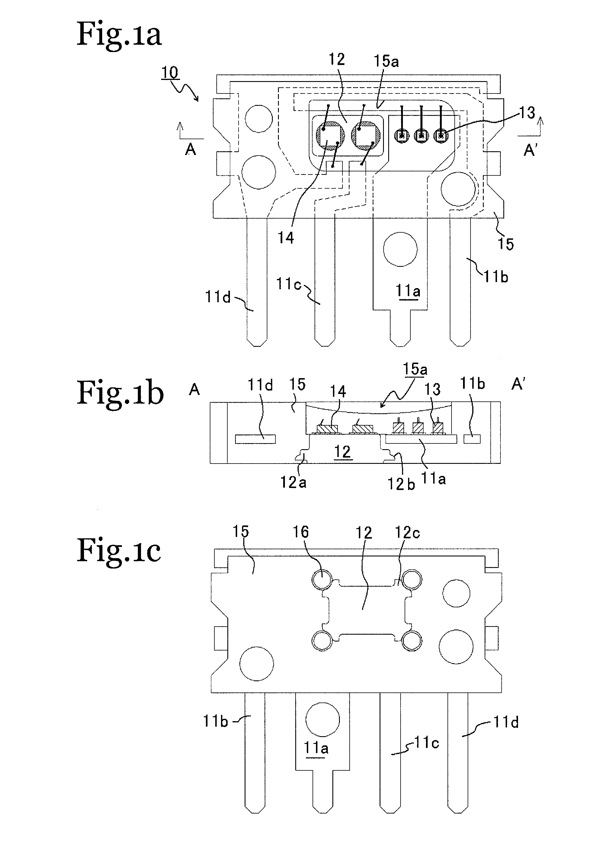
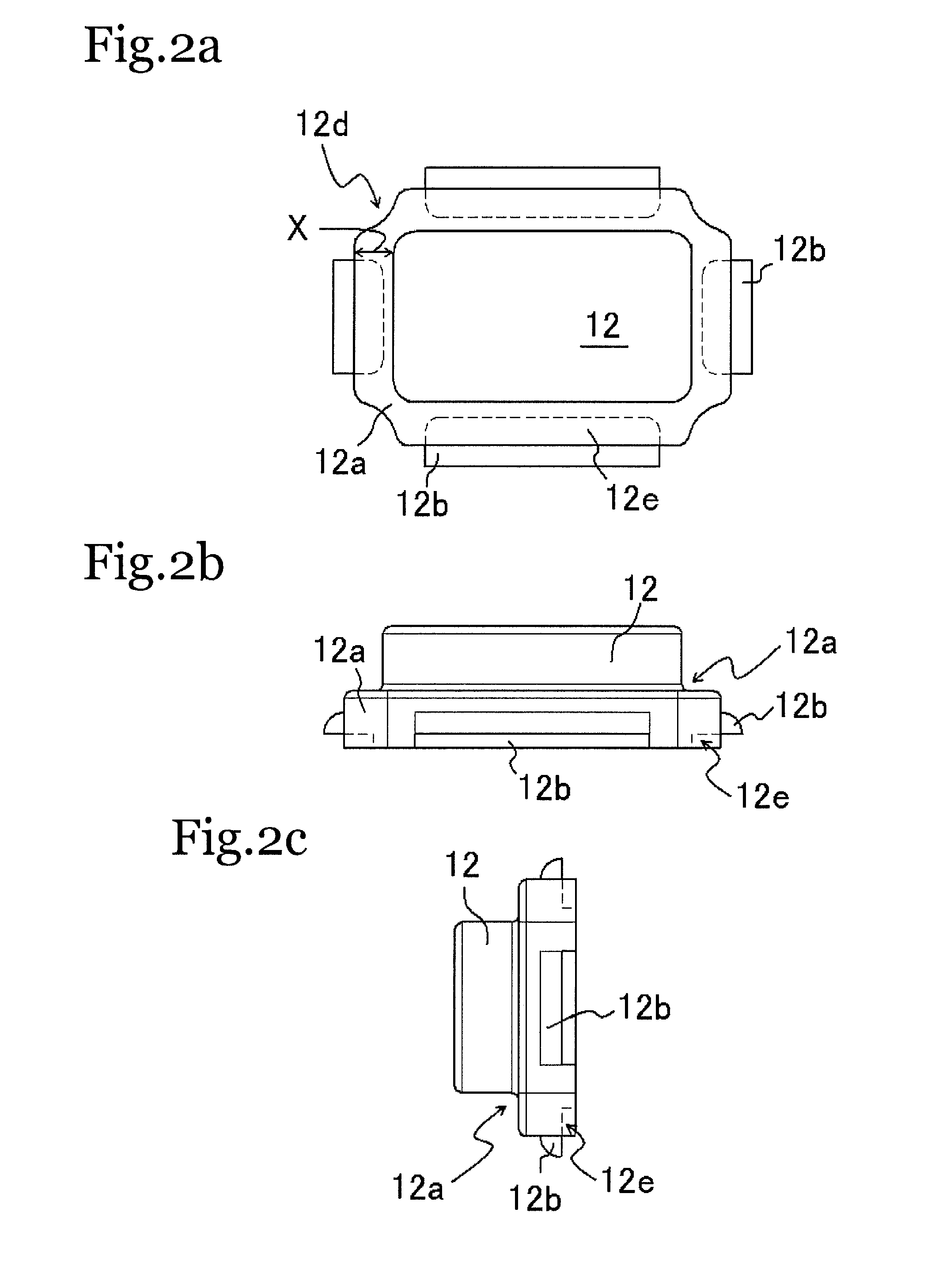
[0039]As shown in FIGS. 1a to 1c, the light emitting device 10 in this example is a side view type light emitting device, in which a first metal member 11a, a second metal member 12, and other metal members 11b to 11d that function as terminals are fixed to a resin package (molding or fixing resin) 15, and ends of these metal members 11a to 11d protrude from one side of the resin package 15.

[0040]The resin package 15 is formed, for example, from PBT, PPA, or another such resin package material that has been used in the past, and its basic shape is a substantially cuboid shape measuring 10×14.5×1.5 mm in size. A window 15a for taking off the light emitted by the light emitting elements (discussed below) is formed on one side of the resin package 15.

[0041]Three light emitting elements 13 that generate relatively little heat are mounted on the first metal member 11a. These light emitting elements 13 are formed from an AlInGaP / GaAs semiconductor that emits red light whose main wavelengt...

example 2

[0062]The constitution of this light emitting device 20 is substantially the same as that of the light emitting device in Example 1, except that, as shown in FIGS. 3a to 3c, it is a top view type of surface-mount light emitting device, in which a first metal member 21a, a second metal member 22, and other metal members 21b to 21d that function as terminals are fixed to a resin package 25, and the other ends of these metal members 21a to 21d protrude from the side faces of the resin package 25 and are bent to function as external terminals.

[0063]With this light emitting device 20, just two diagonally opposed recesses 26 are disposed corresponding to the cut-outs of the second metal member 22 on the back side of the resin package 25.

[0064]This constitution of the light emitting device has substantially the same effect as that of light emitting device of Example 1.


PUM


Abstract

A light emitting device, comprises: a first semiconductor light emitting element; a second semiconductor light emitting element; a first metal member mounting on its top face the first semiconductor light emitting element; a second metal member mounting on its top face the second semiconductor light emitting element; and a resin package having on its top face a window through which light is taken off from the first semiconductor light emitting element and the second semiconductor light emitting element, wherein the second metal member is thinner around its peripheral edge than in its middle, and the rear face of the first metal member is facing the top face of the peripheral edge.

Description

BACKGROUND OF THE INVENTION[0001]1. Field of the Invention[0002]The present invention relates to a light emitting device, and more particularly relates to a light emitting device using a light emitting element such as a light emitting diode.[0003]2. Background Information[0004]Information terminal devices featuring semiconductor light emitting elements occupy an important position today as optical printers and so forth. In particular, full-color printing has become possible with the development of conductor light emitting elements capable of emitting RGB (red, green, and blue) at high brightness levels for all colors. For example, there is a known light emitting device in which a red LED, a green LED, and a blue LED are each mounted on a lead frame, and these lead frames are insulated a specific distance apart. With a light emitting device such as this, however, the lead frames have to be kept apart so they do not touch each other, so the elements have to be disposed away from each ...

Claims


Application Information

Patent Timeline
Patent Type & Authority Applications(United States)
IPC IPC(8): H01L33/00H01L33/64
CPCH01L25/0753H01L33/642H01L33/647H01L2224/48091H01L2224/73265H01L2924/01322H01L2924/00014H01L2924/00
Inventor SUMITANI, NAOFUMI
Owner NICHIA CORP
Why Eureka
Try Eureka