Semiconductor device including microstrip line and coplanar line

a technology of semiconductor devices and microstrip lines, which is applied in the direction of semiconductor devices, semiconductor/solid-state device details, electrical apparatus, etc., can solve the problems of increasing the manufacturing cost of the interconnect substrate and the manufacturing cost of the semiconductor device provided therewith, and achieve the effect of reducing the number of interconnect layers of the interconnect substra

Inactive Publication Date: 2008-06-05
RENESAS ELECTRONICS CORP
View PDF24 Cites 53 Cited by
  • Summary
  • Abstract
  • Description
  • Claims
  • Application Information

AI Technical Summary

Benefits of technology

[0008]In the semiconductor device of the present invention, the transmission line provided on the interconnect substrate and the ground plane provided in the circuit component constitute the microstrip line. Therefore, it is unnecessary to provide a ground plane, which constitutes the microstrip line, in the interconnect substrate. As a result, the number of interconnect layers of the interconnect substrate can be reduced.

Problems solved by technology

This causes an increase in a manufacturing cost of the interconnect substrate, resulting in the increase in the manufacturing cost of a semiconductor device provided therewith.

Method used


Image

  • Semiconductor device including microstrip line and coplanar line
  • Semiconductor device including microstrip line and coplanar line
  • Semiconductor device including microstrip line and coplanar line

Examples


first embodiment

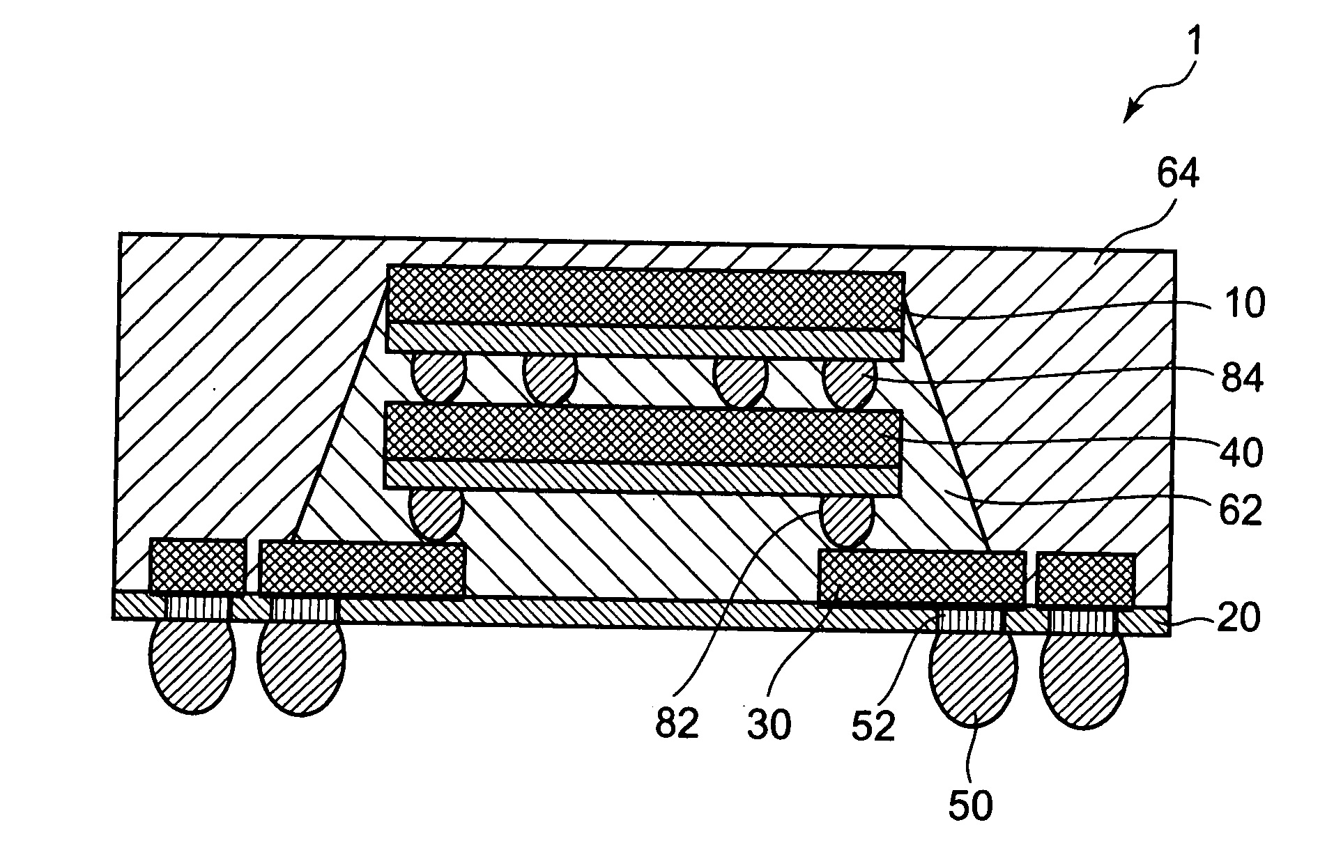
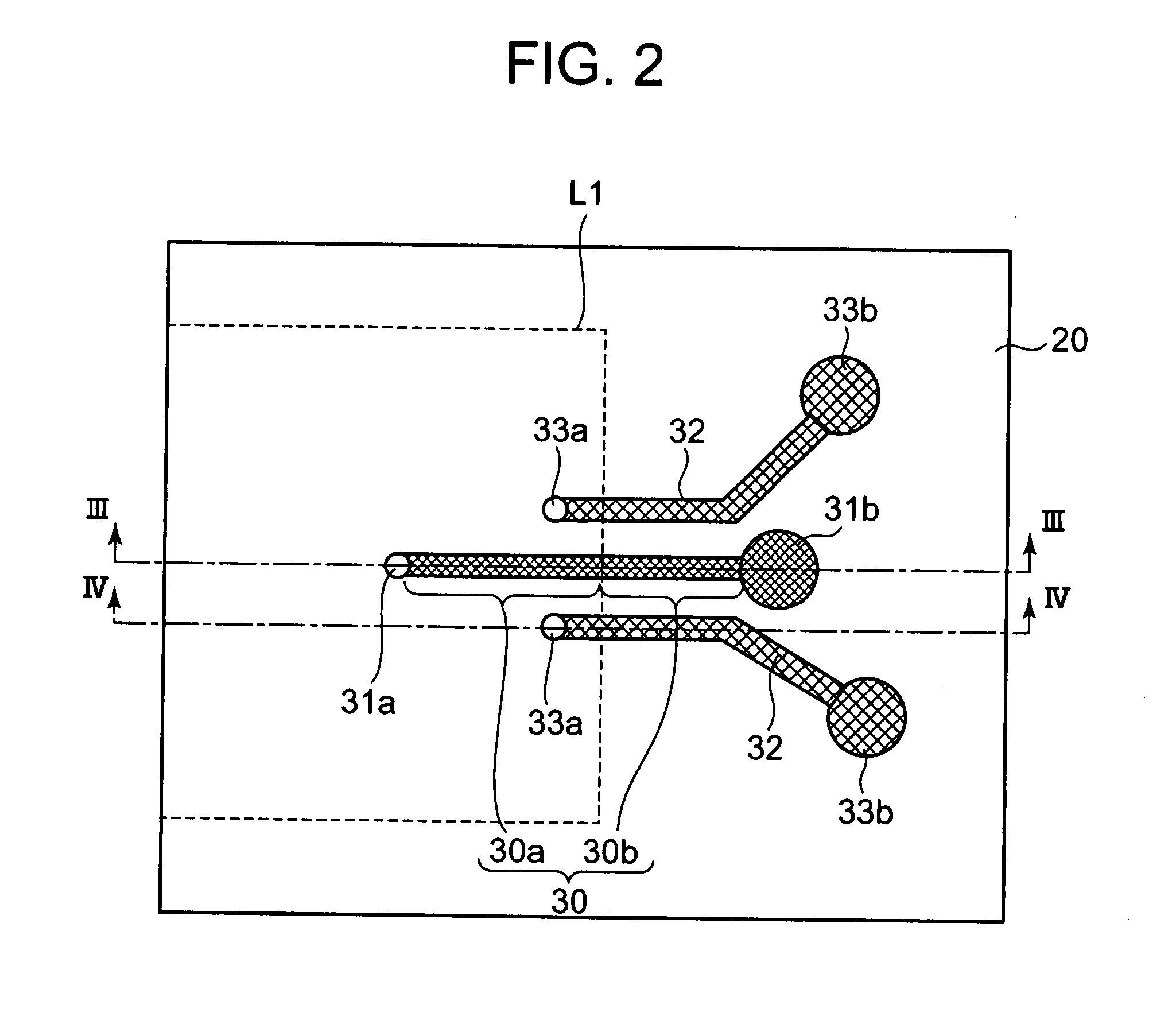
[0039]FIG. 1 is a cross sectional view showing a semiconductor device according to a first embodiment of the present invention. A semiconductor device 1 is a ball grid array (BGA) package which includes a semiconductor chip 10, a package substrate (interconnect substrate) 20, transmission lines 30, and a dummy chip (circuit component) 40. The transmission lines 30 are provided on an upper surface (first main surface) of the package substrate 20. The transmission lines 30 are used to transmit signals from the semiconductor chips 10. The transmission lines 30 are impedance-matched.

[0040]The dummy chip 40 is mounted on the upper surface of the package substrate 20 through flip-chip bonding. In other words, the dummy chip 40 is mounted on the upper surface of the package substrate 20 through conductive bumps 82. The conductive bumps 82 are connected with the transmission lines 30. A gap between the dummy chip 40 and the package substrate 20 is filled with an underfill resin 62. In this ...

second embodiment

[0060]FIG. 10 is a cross sectional view showing a semiconductor device according to a second embodiment of the present invention. A basic structure of the semiconductor device 2 shown in FIG. 10 is approximately the same as the semiconductor device 1 described in the first embodiment. The semiconductor device 2 has the semiconductor chip 10 (first semiconductor chip) and a semiconductor chip 70 (second semiconductor chip). The semiconductor device 2 is different from the semiconductor device 1 in that a semiconductor chip 70 is mounted on the lower surface of the package substrate 20 through flip-chip bonding. In other words, the semiconductor chip 70 is mounted on the lower surface of the package substrate 20 through conductive bumps 72. The semiconductor chip 70 is electrically connected to the semiconductor chip 10 through the conductive bumps 72, the conductive plugs 52 and the conductive bumps 82. A gap between the semiconductor chip 70 and the package substrate 20 is filled wi...

third embodiment

[0064]FIG. 12 is a cross sectional view showing a semiconductor device according to a third embodiment of the present invention. A basic structure of the semiconductor device 3 shown in FIG. 12 is approximately the same as the semiconductor device 1 described in the first embodiment. The semiconductor device 3 is different from the semiconductor device 1 in that a semiconductor chip 70 is mounted on the lower surface of the package substrate 20 through flip-chip bonding, and the semiconductor chip 10 comprises a plurality of semiconductor chips which are stacked on the dummy chip 40.

[0065]The plurality of semiconductor chips 10 are provided and stacked on each other. A gap between a lowermost one of the semiconductor chips 10 and the dummy chip 40 and a gap between adjacent two of the semiconductor chips 10 are filled with the underfill resin 62. A seal resin 64 is provided to cover the semiconductor chips 10 and the dummy chip 40.

[0066]In this embodiment, a semiconductor chip 70 is...


PUM


Abstract

Provided is a semiconductor device including an interconnect substrate, a transmission line which is formed on the interconnect substrate, and a circuit component which is mounted over the interconnect substrate and has a ground plane. The transmission line includes a first portion and a second portion that is connected to the first portion. The first portion and the ground plane constitute a microstrip line. The second portion and ground line constitute a coplanar line.

Description

BACKGROUND OF THE INVENTION[0001]1. Field of the Invention[0002]The present invention relates to a semiconductor device.[0003]2. Description of the Related Art[0004]JP 2003-282782 A discloses an interconnect substrate including a microstrip line. A transmission line for transmitting signals from an IC chip and a ground layer are provided to the interconnect substrate. The transmission line and the ground layer constitute the microstrip line.[0005]Examples of related art documents which are pertinent to the present invention include JP 2001-035957 A and JP 2000-195988 A in addition to JP 2003-282782 A described above.[0006]However, the transmission line and the ground layer which constitute the microstrip line are provided in different layers. Accordingly, the number of interconnect layers increases in the interconnect substrate. This causes an increase in a manufacturing cost of the interconnect substrate, resulting in the increase in the manufacturing cost of a semiconductor device...

Claims


Application Information

Patent Timeline
Patent Type & Authority Applications(United States)
IPC IPC(8): H01L23/48
CPCH01L2924/14H01L2224/73204H01L2924/1532H01L2924/19032H01L2924/19043H01L2924/19103H01L2924/19105H01L2924/30105H01L2924/3011H01L2924/15311H01L2924/01006H01L2924/01005H01L2924/01082H01L21/561H01L21/568H01L23/3128H01L23/3135H01L23/66H01L24/97H01L25/0657H01L2223/6627H01L2224/16145H01L2224/97H01L2225/06517H01L2225/06527H01L2225/06572H01L2924/01029H01L2924/01033H01L2924/01046H01L2924/01047H01L2924/01078H01L2924/01079H01L2224/81H01L2924/15192H01L2924/18161H01L2924/00014H01L2224/81005H01L2924/00011H01L2224/0401
Inventor SOEJIMA, KOJIKAWANO, MASAYAKURITA, YOICHIRO
Owner RENESAS ELECTRONICS CORP
Why Eureka
Try Eureka