Semiconductor memory device
a memory device and semiconductor technology, applied in the field of semiconductor memory devices, can solve the problems of difficult to ensure difficulty in ensuring data retention characteristics of memory cells, and frequent refresh operation of two word lines at every refresh interval, so as to reduce consumption current, suppress the influence of noise, and reduce the average current and peak current in the refresh operation.
- Summary
- Abstract
- Description
- Claims
- Application Information
AI Technical Summary
Benefits of technology
Problems solved by technology
Method used
Image

Examples
first embodiment
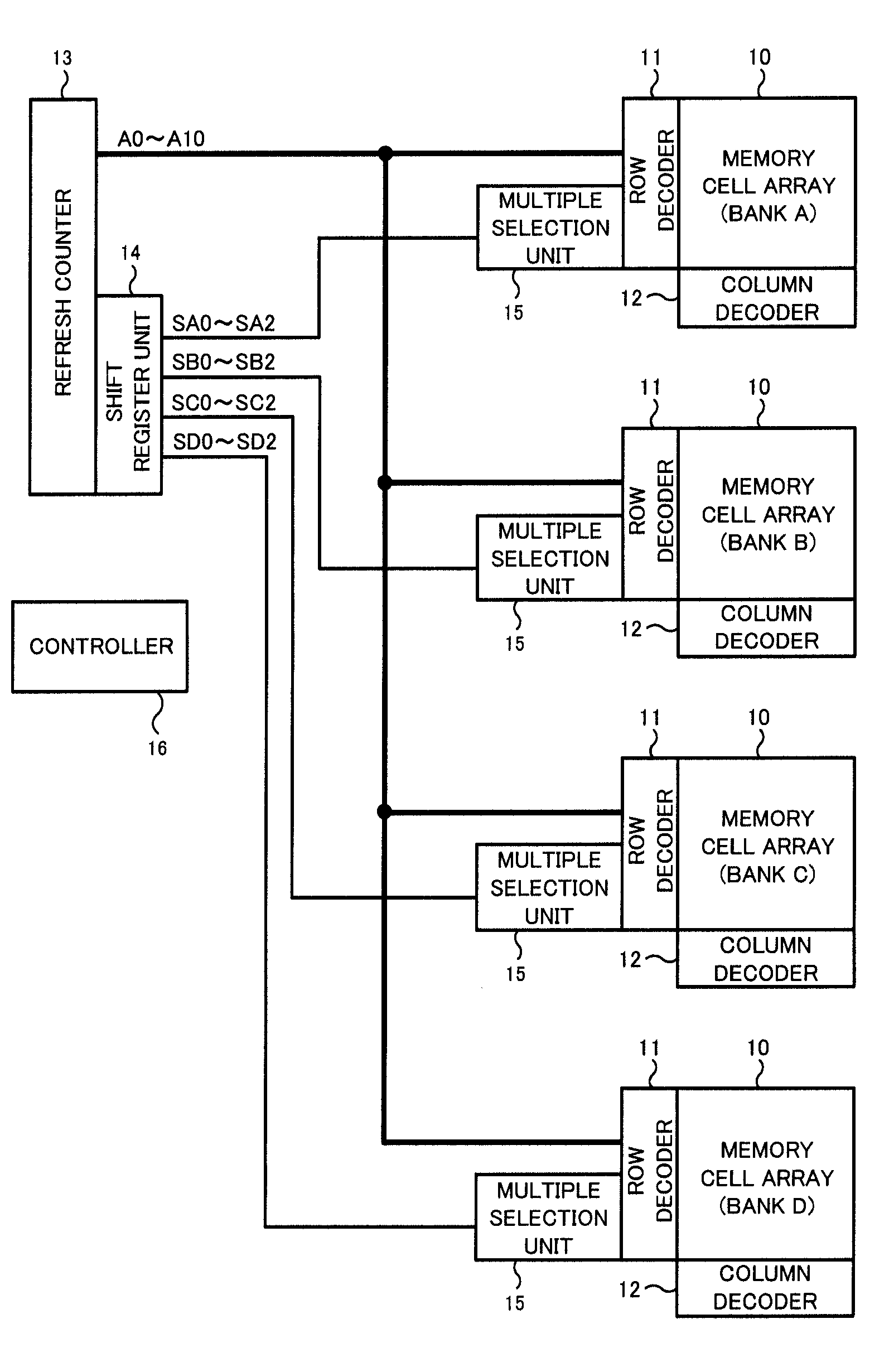
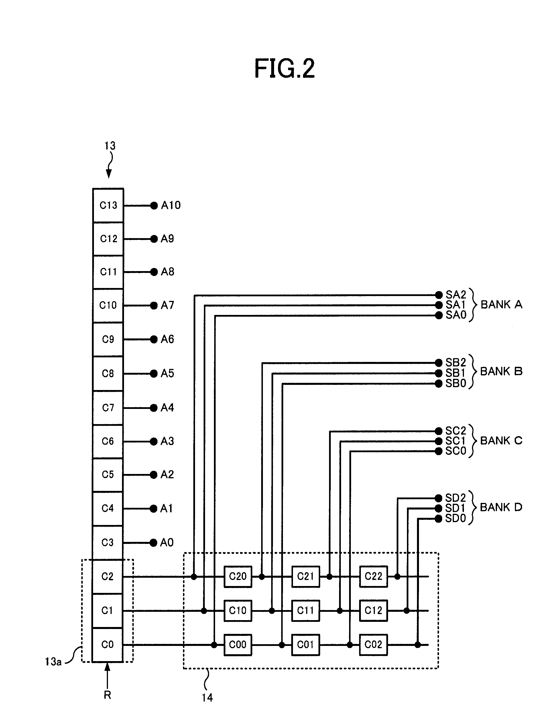
[0031]Configuration and operation of DRAM of a first embodiment will be described first. FIG. 1 is a block diagram showing a principal configuration of the DRAM of the first embodiment. In the DRAM as shown in FIG. 1, a memory cell array 10 including many memory cells is arranged to be divided into four banks. The respective banks denoted as banks A, B, C and D of the memory cell array 10 has the same storage capacity and the same configuration. The memory cell array 10 includes many memory cells formed at intersections between a plurality of word lines and a plurality of bit lines arranged in a matrix form. Read and write operations for the four banks A, B, C and D can be controlled individually. A bank selection signal for selecting the four banks in normal operation is input from outside.
[0032]Row decoders 11 and column decoders 12 are arranged on the periphery of the memory cell array 10 corresponding to the four banks. Each row decoder 11 selects a word line corresponding to a ...
second embodiment
[0056]Next, configuration and operation of DRAM of a second embodiment will be described. FIG. 9 is a block diagram showing a principal configuration of the DRAM of the second embodiment. In the configuration of FIG. 9, a memory cell array 10 divided into four banks A, B, C and D, row decoders 11, column decoders 12 and a controller 16 are the same as those in FIG. 1 of the first embodiment. Meanwhile, there are provided a refresh counter 20 and an address converting unit 21 in FIG. 9, which are constituent elements corresponding to the refresh counter 13, the shift register unit 14 and the multiple selection units 15.
[0057]The refresh counter 20 sequentially outputs a count value corresponding to a row address of a word line to be selected as a refresh target, as in FIG. 1. However, it is different from FIG. 1 in that upper 12 bits of the count value is supplied to each bank as lower 12 bits (A0 to A11) of the row address. Further, lower two bits of the count value of the refresh c...
PUM
 Abstract
Description
Claims
Application Information
 - R&D Engineer
- R&D Manager
- IP Professional
- Industry Leading Data Capabilities
- Powerful AI technology
- Patent DNA Extraction
Browse by: Latest US Patents, China's latest patents, Technical Efficacy Thesaurus, Application Domain, Technology Topic.
© 2024 PatSnap. All rights reserved.Legal|Privacy policy|Modern Slavery Act Transparency Statement|Sitemap