Systems and Methods with Reduced Reference Spurs Using a Crystal Oscillator For Broadband Communications

a crystal oscillator and broadband communication technology, applied in oscillator generators, pulse automatic control, electrical equipment, etc., can solve the problems of reducing reducing the performance of integrated receivers, and limiting the overall receiver sensitivity, so as to achieve the effect of increasing the gain at startup

Active Publication Date: 2008-06-19
NXP BV
View PDF6 Cites 17 Cited by
  • Summary
  • Abstract
  • Description
  • Claims
  • Application Information

AI Technical Summary

Benefits of technology

[0013]Another embodiment of such a system comprises a crystal oscillator circuit comprising: means for limiting an oscillation amplitude of the circuit to a programmable level; and means for providing increased gain at startup such that drive level dependency variation in a crystal of the circuit is compensated.

Problems solved by technology

Secondly, the crystal oscillators should provide a signal output with high peak-to-peak amplitude and low-phase noise.
Reference spurs result in the deterioration of the performance of integrated receivers.
For example, in a fully integrated silicon tuner, reference spurs limit the overall receiver sensitivity and may prevent compliance with many TV standards, including Digital Video Broadcasting-Terrestrial (DVB-T) and Advanced Television Systems Committee (ATSC).
The Pierce crystal oscillator has two perceived drawbacks when used for applications in broadband silicon tuner products.
Firstly, such an oscillator does not possess an Automatic Level Control (ALC) feedback loop for controlling the amplitude of the reference signals.
This design of the loop gain pushes the amplifier of the Pierce crystal oscillator deeper into compression for nominal crystals, generating much higher spurious harmonic content in the switching currents.
These reference spurs then fall within the signal band of the tuner and limit the overall sensitivity of the receiver.
Secondly, the Pierce crystal oscillator has a single-ended design, which tends to generate high switching currents and large transient currents over a portion of the oscillation cycle during the discharging of the crystal.
Firstly, the analog ALC circuit has many noise sources such as transistors, resistors and additional current sources, which raise the phase noise of the analog ALC crystal oscillator, and consequently the integrated phase noise of the phase-locked loop.

Method used


Image

  • Systems and Methods with Reduced Reference Spurs Using a Crystal Oscillator For Broadband Communications
  • Systems and Methods with Reduced Reference Spurs Using a Crystal Oscillator For Broadband Communications
  • Systems and Methods with Reduced Reference Spurs Using a Crystal Oscillator For Broadband Communications

Examples


Embodiment Construction

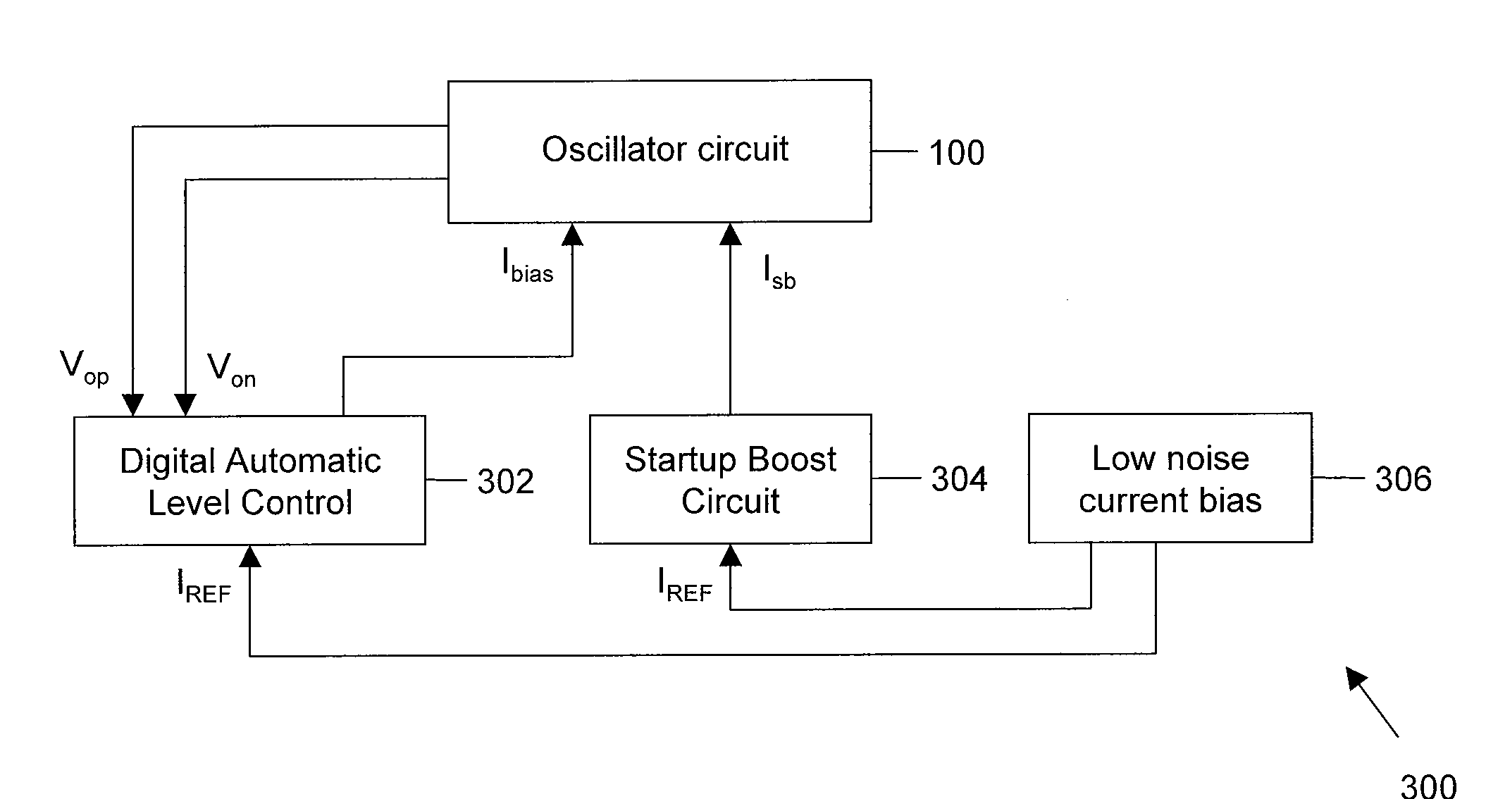
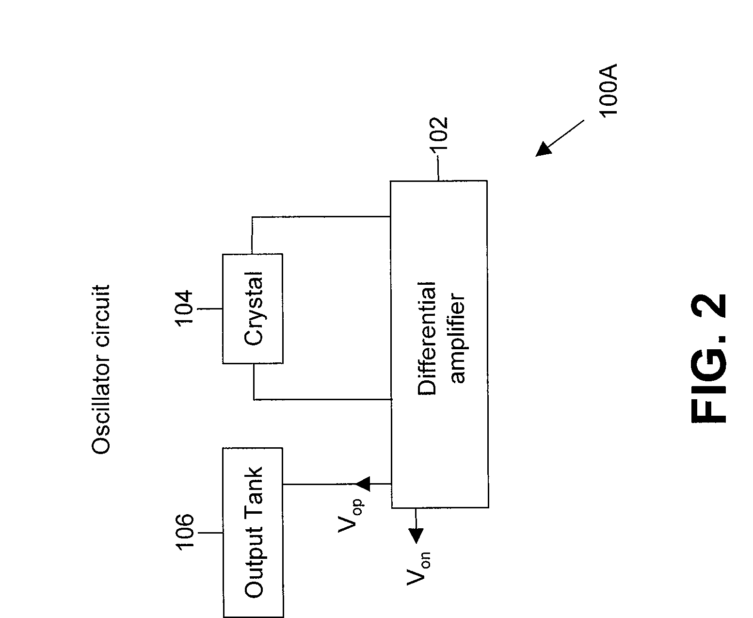
[0034]Exemplary embodiments involve crystal oscillator circuits that can be configured to provide reference signals in broadband chip sets. Such an oscillator circuit can include a differential amplifier, a digital automatic level control circuit, and a startup boost circuit. The differential amplifier provides differential output signals with reduced reference spurs. The DALC provides feedback control on the amplitude of the reference signals, while adding less phase noise, as compared to analog Automatic Level Control (ALC) circuits. The start up boost circuit compensates for the drive-level dependencies of the crystal. The reference signals provided by the oscillator circuit have reduced harmonic content and phase noise, as compared to oscillator circuits in the prior art.

[0035]The individual circuit blocks may be used independently or in any combination to reduce the reference spurs when integrated on the same die as a receiver.

[0036]FIG. 1 is a block diagram of an embodiment of...


PUM


Abstract

Systems and methods are provided. In this regard, a representative system incorporates a crystal oscillator circuit and a digital automatic level control circuit. The digital automatic level control circuit is operative to: convert an oscillation amplitude of the crystal oscillator circuit to a proportional DC voltage; convert the DC voltage to a corresponding digital code representation; and adjust bias current and oscillator loop gain such that a desired oscillation amplitude is set.

Description

TECHNICAL FIELD[0001]The invention generally relates to crystal oscillator circuits and the devices in which such circuits operate or with which such circuits are associated.DESCRIPTION OF THE RELATED ART[0002]A crystal oscillator is an electronic circuit that uses the mechanical resonance of a physical crystal of piezoelectric material, along with an amplifier and feedback, to create an electrical signal at a very precise frequency. The loop gain of a crystal oscillator is the amount of amplification brought about in the electrical signal in the closed loop of the amplifier and feedback paths.[0003]Crystal oscillators are used for providing very precise reference signals to phase locked-loops used in broadband communication chip sets. The crystal oscillator may be integrated onto the same substrate as one or more of the dies in the chip set, including the tuner and / or demodulator, thereby providing highly integrated broadband communication chip sets.[0004]The design of crystal osci...

Claims


Application Information

Patent Timeline
Patent Type & Authority Applications(United States)
IPC IPC(8): H03B5/32
CPCH03B5/06H03L3/00H03B5/364
Inventor ROSIK, RAYGAO, WEINANLINDSTROM, MATS
Owner NXP BV
Why Eureka
Try Eureka