Method of forming a low-k dual damascene interconnect structure

a damascene and interconnecting structure technology, applied in the direction of basic electric elements, semiconductor/solid-state device manufacturing, electric apparatus, etc., can solve the problems of difficult processing of low-k dielectric materials, complex integrated circuits, and complex devices, so as to improve the adhesion of the structure

Inactive Publication Date: 2008-06-19
APPLIED MATERIALS INC
View PDF25 Cites 23 Cited by
  • Summary
  • Abstract
  • Description
  • Claims
  • Application Information

AI Technical Summary

Benefits of technology

[0013]The present invention generally relates to a method of etching a low K dielectric material and, in particular, to the formation of low K dielectric dual damascene interconnect structures. A method of etching a low K dielectric material comprises hardening a portion of a low K dielectric, then etching non-hardened portions of the material. The invention further includes a method of fabricating an interconnect structure comprising etching a via into an upper low K dielectric layer and into a hardened portion of a lower low K dielectric layer. The via is defined by a pattern formed in a photoresist layer. The photoresist layer is then stripped, and a trench that circumscribes the via as defined by a hard mask is etched into the upper low K dielectric layer and, simultaneously, the via that was etched into the hardened portion of the lower low K dielectric layer is further etched into the lower low K dielectric layer. The result is a low K dielectric dual damascene structure. Alternatively, a mask etching step may be provided between the first via etch and the trench etch. The mask etching step is used to correct any misalignment of the trench and via patterns. Furthermore, in another embodiment of the invention, adhesion of the structure is improved by plasma treating a low K barrier layer prior to depositing the low K dielectric material upon the low K barrier layer.

Problems solved by technology

Integrated circuits have evolved into complex devices that can include millions of components (e.g., transistors, capacitors and resistors) on a single chip.
Capacitive coupling between adjacent metal interconnects may cause cross talk and / or resistance-capacitance (RC) delay which degrades the overall performance of the integrated circuit.
Unfortunately, low K dielectric materials are not easy to process using damascene and dual damascene techniques.
In particular, low K dielectric materials are susceptible to damage during plasma processing, such as plasma etching used to strip photoresist layers after the low K dielectric layer has been etched.
Furthermore, low K dielectrics are prone to have adhesion problems, i.e., the low K materials do not effectively adhere to underlying layers.
The process of the prior art is fraught with difficulties.
The use of a cap layer to protect the low K dielectric during trench etch complicates the process by requiring additional deposition and etch processing.
Also, it is difficult to find suitable etch stop layers and hard mask layers that have both good etch selectivity with respect to the low K dielectric layer and sufficiently low dielectric constants themselves.
Furthermore, it is difficult to achieve these goals without creating a process that is overly complex or requires the use of numerous processing chambers.

Method used


Image

  • Method of forming a low-k dual damascene interconnect structure
  • Method of forming a low-k dual damascene interconnect structure
  • Method of forming a low-k dual damascene interconnect structure

Examples


Embodiment Construction

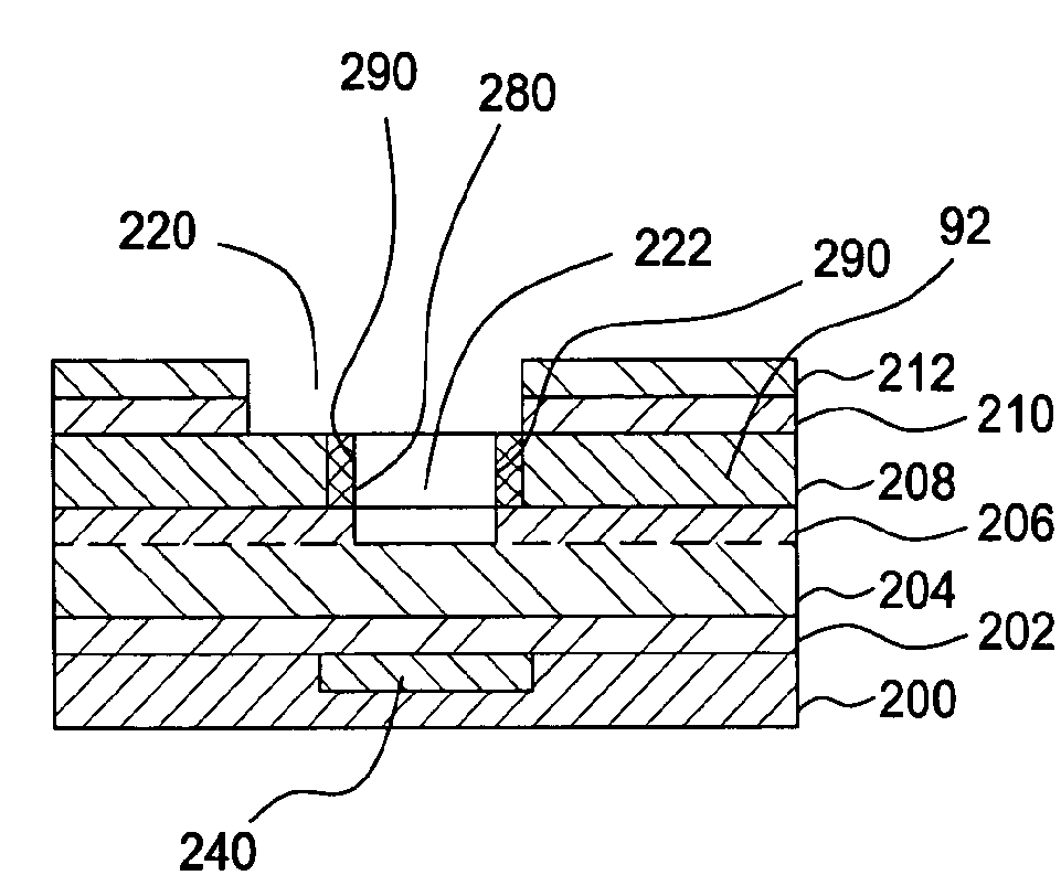
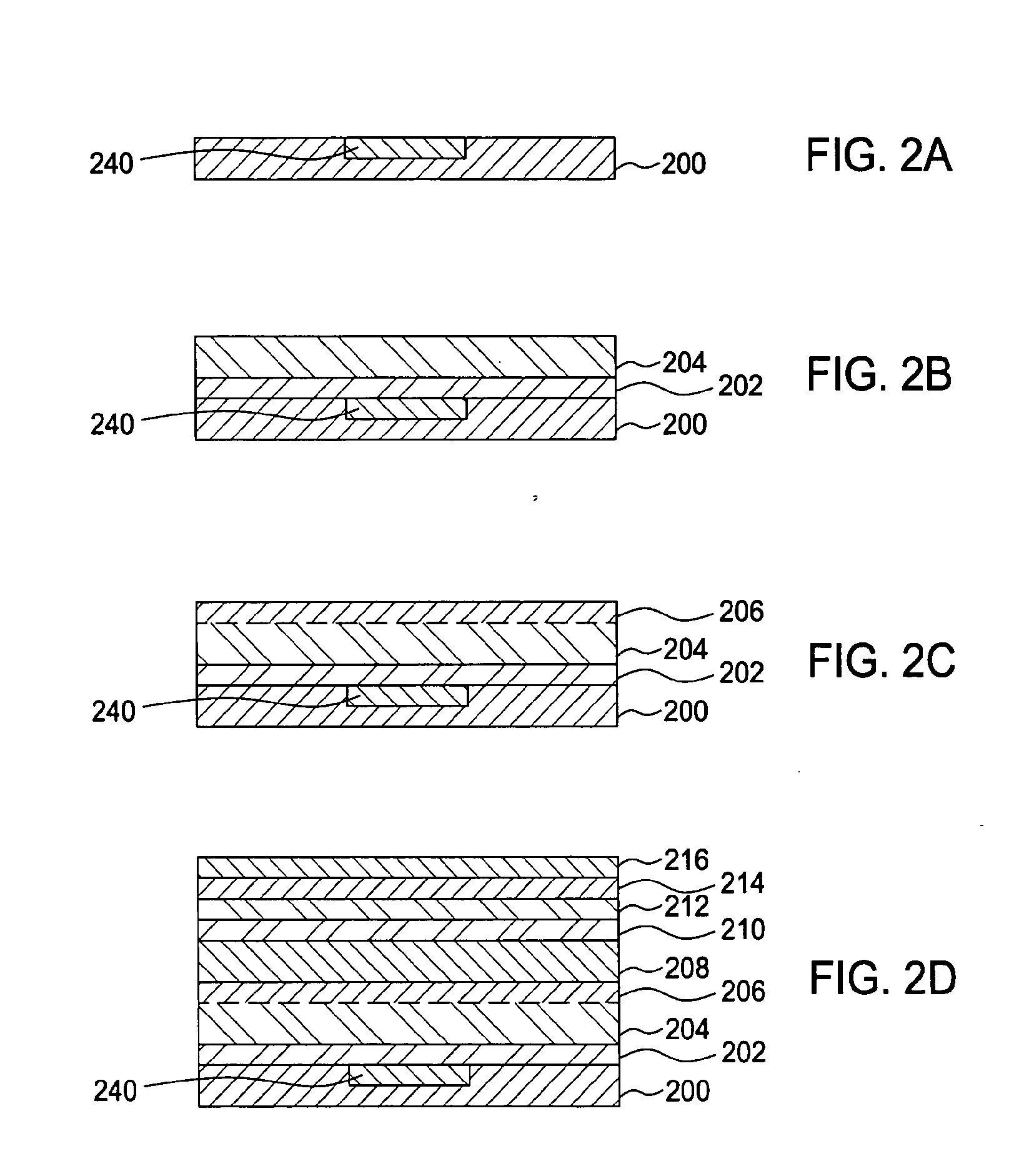
[0020]The present invention relates to a method of etching a low K dielectric material and, in particular, to fabricating a dual damascene interconnect structure comprising dielectric materials having lower dielectric constants (low K). The structure is formed by etching a via in an upper low K dielectric layer and into a hardened portion of a lower low K dielectric layer, then simultaneously etch a trench in the upper low K dielectric layer and a via in the lower low K dielectric layer. The hardened portion forms a mask for the via and a hard mask forms a mask for the trench. In one embodiment, adhesion of the structure to underlying layer(s) is improved by plasma treating a barrier layer for the structure.

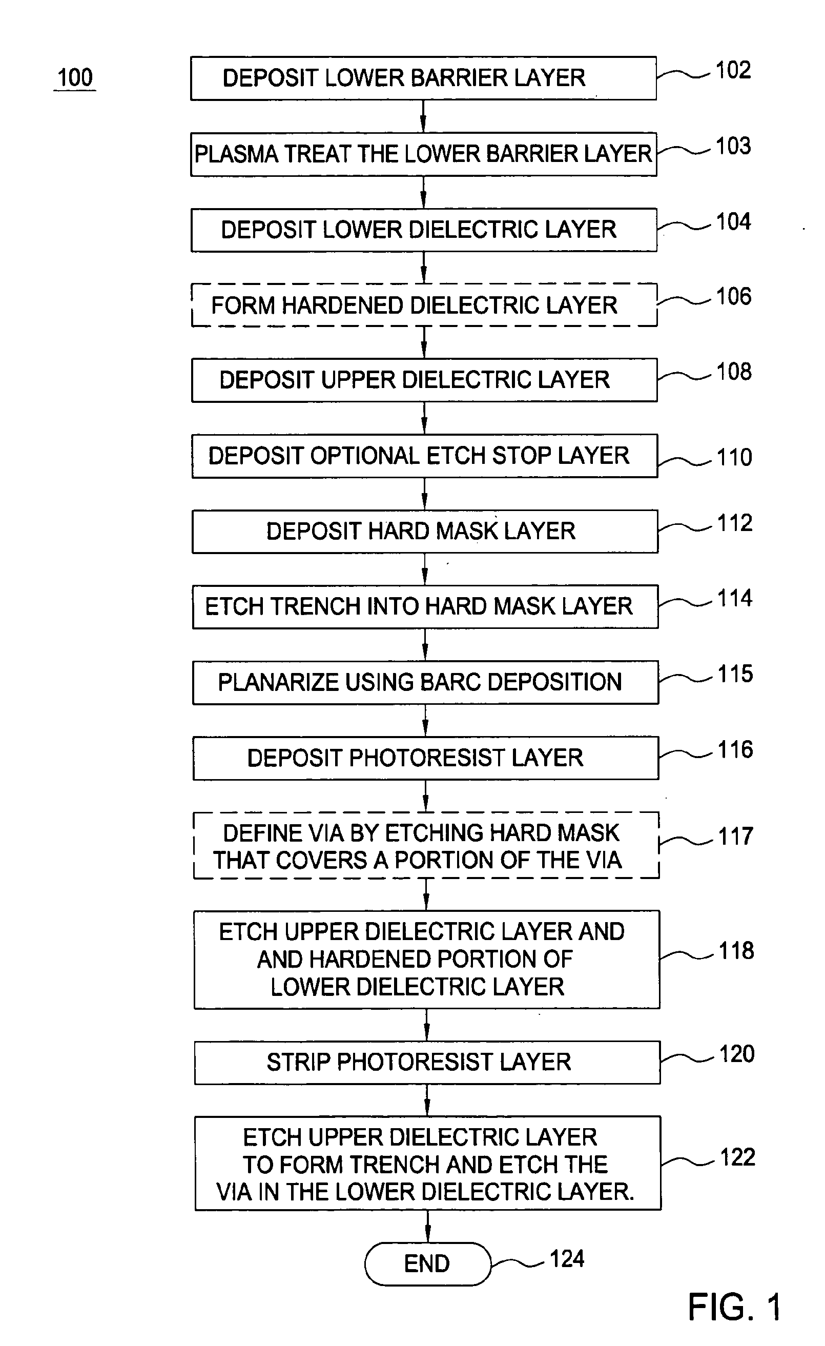
[0021]FIG. 1 depicts a sequence 100 of method steps that may be used to form a low-K dual damascene structure according to one embodiment of the invention. The sequence 100 comprises depositing a lower barrier layer on a substrate (step 102), plasma treating the lower barrier lay...


PUM

PropertyMeasurementUnit
dielectric constantaaaaaaaaaa
pressureaaaaaaaaaa
temperatureaaaaaaaaaa

Abstract

A method of fabricating an interconnect structure comprising etching a via into an upper low K dielectric layer and into a hardened portion of a lower low K dielectric layer. The via is defined by a pattern formed in a photoresist layer. The photoresist layer is then stripped, and a trench that circumscribes the via as defined by a hard mask is etched into the upper low K dielectric layer and, simultaneously, the via that was etched into the hardened portion of the lower low K dielectric layer is further etched into the lower low K dielectric layer. The result is a low K dielectric dual damascene structure.

Description

CROSS-REFERENCE TO RELATED APPLICATIONS[0001]This application is a divisional of co-pending U.S. patent application Ser. No. 10 / 745,344, filed Dec. 22, 2003, which claims benefit of U.S. provisional patent application Ser. No. 60 / 437,472, filed Dec. 31, 2002. Each of the aforementioned related patent applications is herein incorporated by reference.BACKGROUND OF THE INVENTION[0002]1. Field of the Invention[0003]The present invention generally relates to a damascene structures for integrated circuits and, more particularly, to a method of forming a dual damascene structure comprising dielectric materials having low dielectric constants (low K).[0004]2. Description of the Related Art[0005]Integrated circuits have evolved into complex devices that can include millions of components (e.g., transistors, capacitors and resistors) on a single chip. The evolution of chip designs continually requires faster circuitry and greater circuit density. The demands for greater circuit density necess...

Claims


Application Information

Patent Timeline
Patent Type & Authority Applications(United States)
IPC IPC(8): H01L21/76H01L21/768
CPCH01L21/76811H01L21/76826H01L21/76813
Inventor DELGADINO, GERARDO A.YE, YANSHIN, NEUNGHOKIM, YUNSANGXIA, LI-QUNHUANG, TZU-FANGHUANG, LIHUA LICHIU, JOEYZHAO, XIAOYETIAN, FANGZHU, WENYIEH, ELLIE
Owner APPLIED MATERIALS INC
Why Eureka
Try Eureka