Electrostatic Discharge Device Verification in an Integrated Circuit

a technology of integrated circuit and electrostatic discharge, which is applied in the direction of error detection/correction, instruments, program control, etc., can solve the problem of not providing sufficient accuracy

Inactive Publication Date: 2008-06-19
BELL SEMICON LLC
View PDF13 Cites 20 Cited by
  • Summary
  • Abstract
  • Description
  • Claims
  • Application Information

AI Technical Summary

Benefits of technology

[0007]The present invention meets the above-noted need by providing, in an illustrative embodiment thereof an automated ESD verification methodology for verifying connectivity and functionality of ESD devices in an IC. These automated checks are based on technology specific electrical rules which are determined by running ESD testers during technology development. The rule-based ESD verification methodologies of the invention replace manual c

Problems solved by technology

The rule-based ESD verification methodologies of the invention replace manual checks which are pr

Method used


Image

  • Electrostatic Discharge Device Verification in an Integrated Circuit
  • Electrostatic Discharge Device Verification in an Integrated Circuit
  • Electrostatic Discharge Device Verification in an Integrated Circuit

Examples


Embodiment Construction

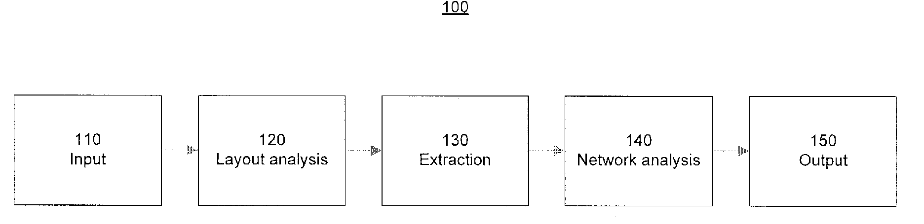
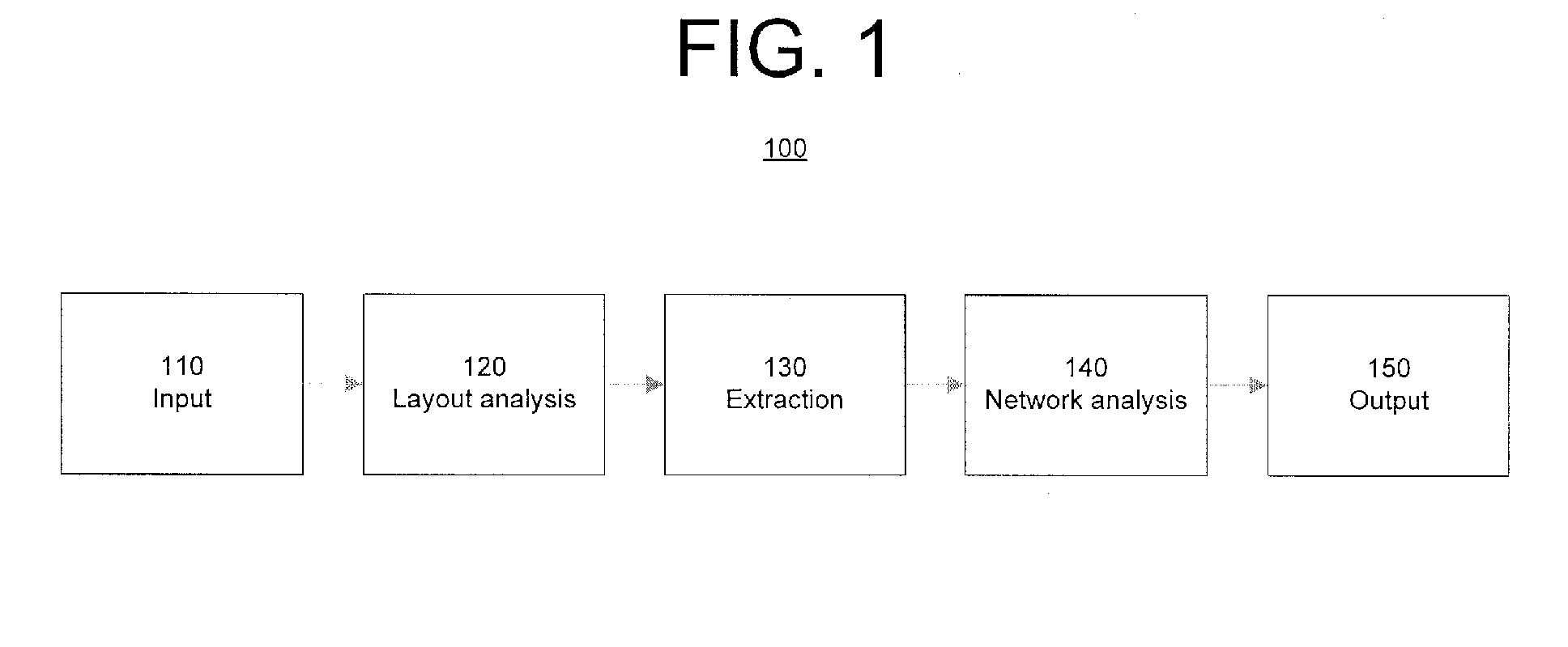
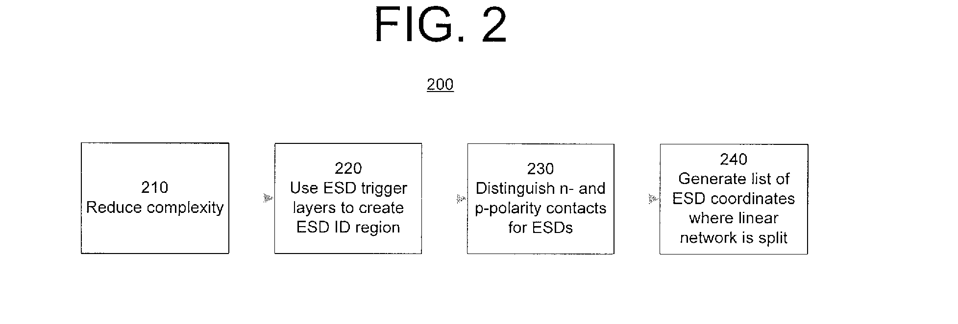
[0018]The present invention will be described herein in the context of an illustrative electronic design automation tool for performing enhanced ESD simulation in an IC. While reference may be made herein to certain ESD circuitry in the IC, it is to be understood that the present invention is not limited to these or any particular ESD circuit arrangements. Rather, the invention is more generally applicable to techniques for advantageously verifying ESD device connectivity and / or functionality in an IC. Techniques of the present invention provide an ESD verification methodology that affords IC designers the freedom to create new I / O topologies optimized for their specific application, without relying on manual verification which is prone to errors. Moreover, the ESD verification methodology of embodiments of the invention is based on a final IC layout and does not require ESD device current-voltage (IV) modeling. Unlike conventional approaches, the present invention takes into accoun...


PUM


Abstract

Computer-implemented techniques for verifying ESD device connectivity in an IC include the steps of: receiving an input dataset including layout parameters corresponding to the integrated circuit; identifying ESD devices based at least in part on the input dataset; extracting devices and parasitic elements in at least a portion of the integrated circuit based at least in part on the input dataset; generating a file including connectivity information and dimensional characteristics for extracted devices and parasitic elements associated with at least ESD protection circuitry in the integrated circuit; identifying at least one ESD test based on the identified ESD devices and on connectivity to the respective ESD devices; and performing a linear network analysis for each identified ESD test based at least in part on the netlist evaluated under ESD conditions, the identified ESD devices being removed from the network analysis, the network analysis being used to ensure that current densities through respective conductive connections included in the identified ESD test are less than or equal to a first prescribed threshold, and/or voltage drops associated with the respective conductive connections are less than or equal to a second prescribed threshold.

Description

FIELD OF THE INVENTION[0001]The present invention relates generally to integrated circuit (IC) testing, and more particularly relates to verifying electrostatic discharge (ESD) device functionality and / or connectivity in an IC.BACKGROUND OF THE INVENTION[0002]Presently, electrical testing of fabricated ICs is used to minimize the number of ESD problems that can occur. Unfortunately, correcting design-related problems discovered in silicon, after IC fabrication, is costly, primarily because of the time and expense of regenerating new reticules and fabricating new silicon. Additionally, IC fabrication delays can disrupt customer production and delivery schedules, thereby increasing costs even further. Consequently, it is desirable to ascertain ESD-related problems earlier in the design cycle, prior to IC fabrication.[0003]One mechanism leading to ESD failure involves insufficient connections to ESD protection devices in the IC (e.g., metal too narrow or insufficient number of conducti...

Claims


Application Information

Patent Timeline
IPC IPC(8): G06F17/50
CPCG06F17/5036G06F30/367
Inventor BELL, DAVID AVERILLLEUNG, CHE CHOIWROGE, DANIEL MARK
Owner BELL SEMICON LLC
Why Eureka
Try Eureka