Apparatus for transferring semiconductor chip and method of transferring semiconductor chip using the same

Active Publication Date: 2008-06-26
SAMSUNG ELECTRONICS CO LTD
View PDF5 Cites 27 Cited by
  • Summary
  • Abstract
  • Description
  • Claims
  • Application Information

AI Technical Summary

Benefits of technology

[0008]The present invention provides an apparatus for transferring a semiconductor chip, which inhibits the occurrence of a void to enhance the reliability of a semiconduc

Problems solved by technology

Thus, when the holder member is inserted into the absorption member, the flatness of a bottom surface of the absorption member may deteriorate.
As a result, air remains between the central portion of the semiconductor ch

Method used


Image

  • Apparatus for transferring semiconductor chip and method of transferring semiconductor chip using the same
  • Apparatus for transferring semiconductor chip and method of transferring semiconductor chip using the same
  • Apparatus for transferring semiconductor chip and method of transferring semiconductor chip using the same

Examples


Example

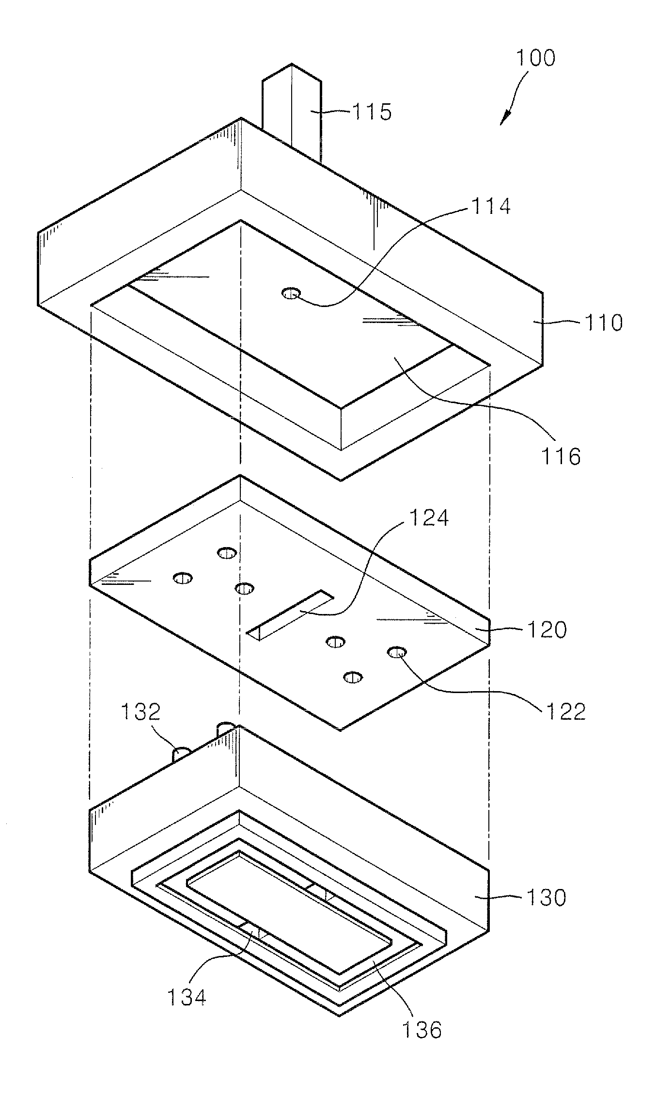
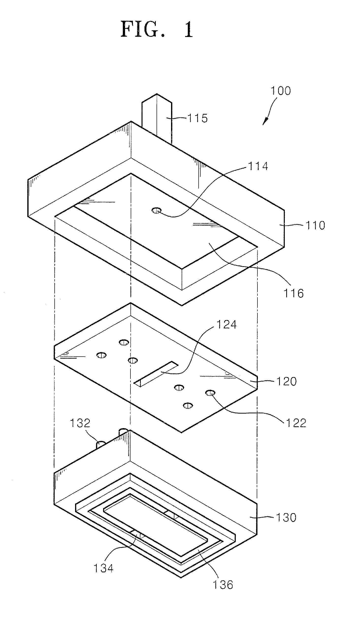
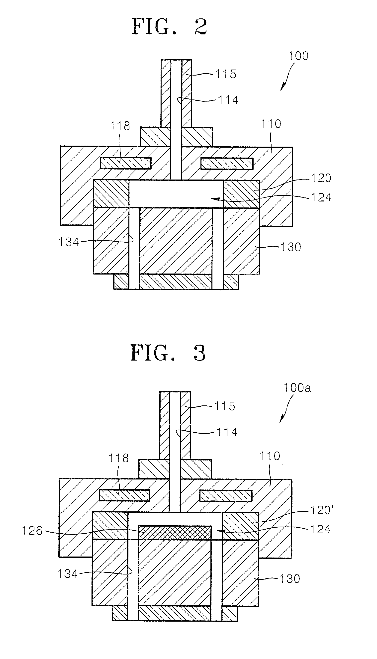
[0017]FIG. 1 is an exploded perspective view of an apparatus 100 for transferring a semiconductor chip according to an embodiment of the present invention, and FIG. 2 is a cross-sectional view of the apparatus 100 for transferring a semiconductor chip shown in FIG. 1.

[0018]Referring to FIGS. 1 and 2, the apparatus 100 for transferring the semiconductor chip may include a holder member 110, a plate member 120, and an absorption member 130. The holder member 110 may function as a body for fixing the plate member 120 and the absorption member 130. The absorption member 130 may pick up a semiconductor chip (not shown) using vacuum and hold the semiconductor chip. The absorption member 130 is combined with the plate member 120, and the plate member 120 is combined with the holder member 110. Vacuum suction may be externally applied to the holder member 110 and then, applied to the absorption member 130 through the plate member 120.

[0019]The holder member 110 may include a vacuum line 115...


PUM

PropertyMeasurementUnit
Timeaaaaaaaaaa
Pressureaaaaaaaaaa

Abstract

Provided are an apparatus for transferring a semiconductor chip and a method of transferring a semiconductor chip using the same, which can inhibit the occurrence of a void to enhance the reliability of a semiconductor package. The apparatus for transferring the semiconductor chip includes: a holder member including a first vacuum hole connected to a vacuum line; a plate member including at least one second vacuum hole corresponding to the first vacuum hole and redistributed to edges of the plate member, the plate member combined with the holder member; and an absorption member including at least one third vacuum hole corresponding to the second vacuum hole and a groove connected to the third vacuum hole, the absorption member combined with the plate member and the holder member.

Description

CROSS-REFERENCE TO RELATED PATENT APPLICATION[0001]This application claims priority under 35 USC § 119 to Korean Patent Application No. 10-2006-0133080, filed on Dec. 22, 2006 in the Korean Intellectual Property Office, the contents of which are incorporated herein in their entirety by reference.BACKGROUND[0002]1. Technical Field[0003]The present invention relates to a semiconductor packaging process, and more particularly, to an apparatus for transferring a semiconductor chip and a method of transferring a semiconductor chip using the same.[0004]2. Description of the Related Art[0005]According to conventional semiconductor manufacturing processes, a plurality of semiconductor chips are fabricated on a wafer at the same time, separated into die units, and packaged separately. For example, wafer-level semiconductor chips are diced into die units and separately attached to a package substrate using an apparatus for transferring semiconductor chips.[0006]A conventional apparatus for tr...

Claims


Application Information

Patent Timeline
IPC IPC(8): H05K7/10H05K13/04B23B31/30
CPCH01L21/6838H05K13/0408Y10T29/49131Y10T29/53191Y10T29/53178Y10T29/5313Y10T29/4913Y10T279/11H05K13/0409H01L21/67H01L21/68
Inventor OH, KOOK-JIN
Owner SAMSUNG ELECTRONICS CO LTD
Why Eureka
Try Eureka