Chip-probing and bumping solutions for stacked dies having through-silicon vias

a technology of throughsilicon vias and stacked dies, which is applied in the field of integrated circuits, can solve the problems of reducing the size of the minimum required to make these components, physical limits of the density that can be achieved in two dimensions, and requiring more complex designs

Inactive Publication Date: 2008-06-26
TAIWAN SEMICON MFG CO LTD
View PDF4 Cites 47 Cited by
  • Summary
  • Abstract
  • Description
  • Claims
  • Application Information

AI Technical Summary

Benefits of technology

[0014]In accordance with yet another aspect of the present invention, a method of probing dies includes providing a stack structure having a first thickness less than a required thickness for a chip probing process, wherein the stack structure comprises a bottom wafer. A handling wafer is attached on the stack structure to increase the first thickness of the stack structure to a second thickness greater than the required thickness. Dies on the stack structure are probed. The handling wafer is removed after the step of probing. Then the stack structure is sawed into separate dies.

Problems solved by technology

Although dramatic improvements in lithography have resulted in considerable improvements in 2D integrated circuit formation, there are physical limits to the density that can be achieved in two dimensions.
One of these limits is the minimum size needed to make these components.
Also, when more devices are put into one chip, more complex designs are required.
An additional limitation comes from the significant increase in the number and length of interconnections between devices as the number of devices increases.
When the number and length of interconnections increase, both circuit resistance-capacitance (RC) delay and power consumption increase.
This results in a structure too thin for the chip probing.
However, the total thickness of 5 mils is not thick enough for the chip probing, which may break the stack structure.
The conflicting requirements for the thicknesses of the stack structure cause a dilemma.

Method used


Image

  • Chip-probing and bumping solutions for stacked dies having through-silicon vias
  • Chip-probing and bumping solutions for stacked dies having through-silicon vias
  • Chip-probing and bumping solutions for stacked dies having through-silicon vias

Examples


Embodiment Construction

[0020]The making and using of the presently preferred embodiments are discussed in detail below. It should be appreciated, however, that the present invention provides many applicable inventive concepts that can be embodied in a wide variety of specific contexts. The specific embodiments discussed are merely illustrative of specific ways to make and use the invention, and do not limit the scope of the invention.

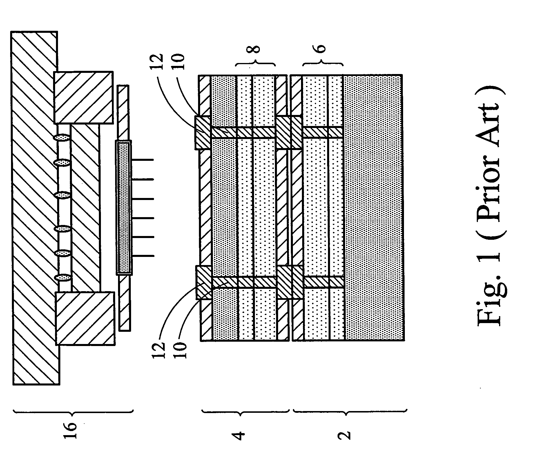
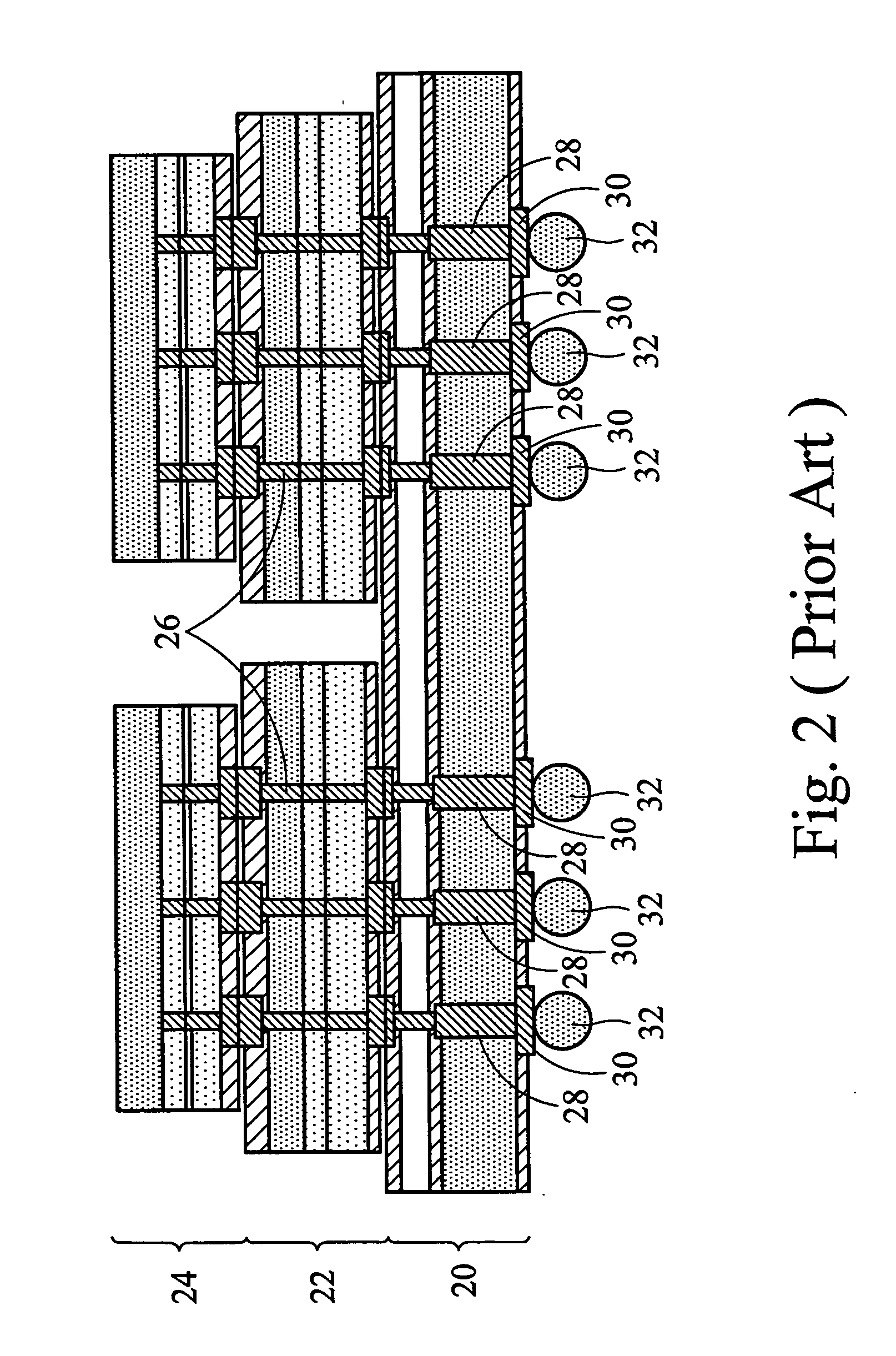
[0021]The cross-sectional views of intermediate stages for forming a three-dimensional integrated circuit (3D IC) are illustrated in FIGS. 3 through 12 and discussed. The variations of the preferred embodiments are then discussed. Throughout the various views and illustrative embodiments of the present invention, like reference numbers are used to designate like elements.

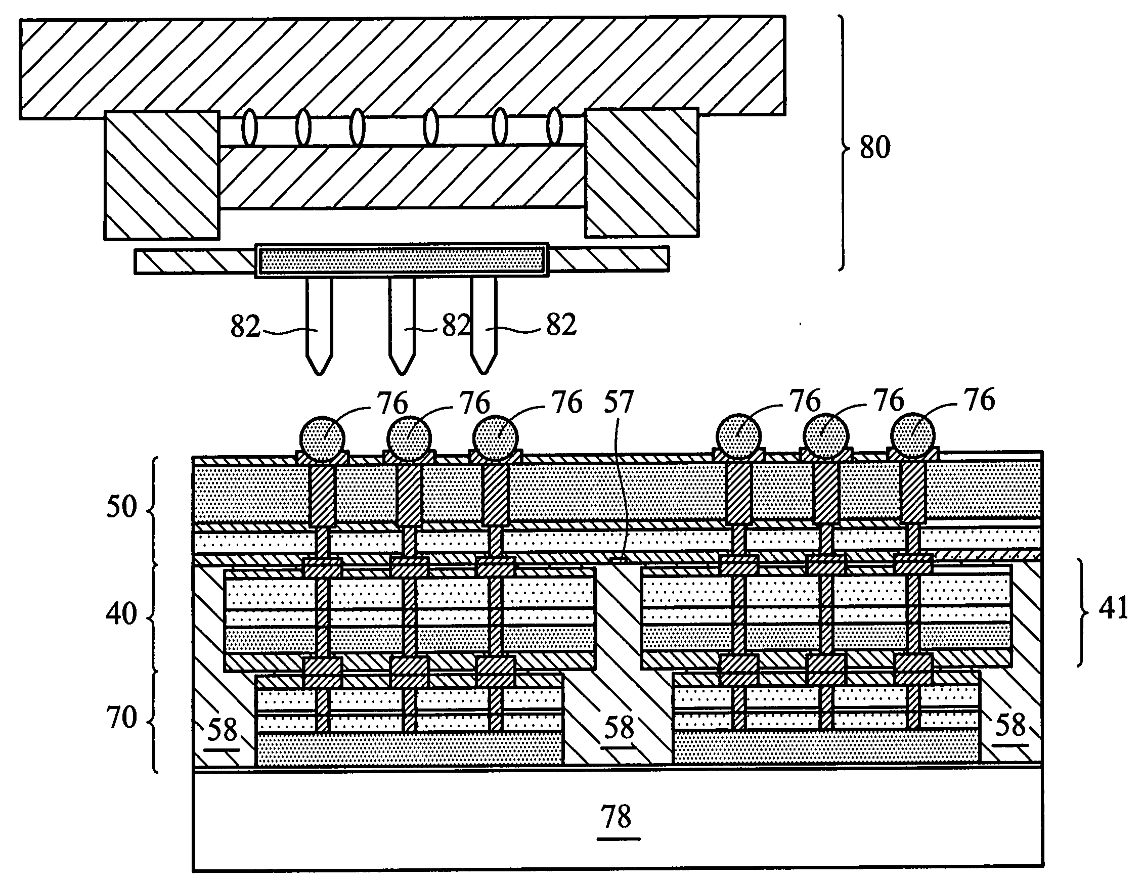
[0022]FIG. 3 illustrates die 40, which will be bonded to a semiconductor wafer. Die 40 includes semiconductor substrate 43, wherein integrated circuits (not shown) are formed at surface 401 of substrate 43. S...


PUM


Abstract

A method of forming a semiconductor structure includes providing a stack structure having a first side and a second side opposite the first side. The stack structure includes a bottom wafer comprising a substrate; a plurality of through-silicon vias in the substrate; and a plurality of under bump metallurgies (UBMs) connected to the plurality of through-silicon vias, wherein the UBMs are on the first side of the stack structure. The method further includes attaching a handling wafer on the second side of the stack structure; performing a chip probing process; and removing the handling wafer from the stack structure.

Description

TECHNICAL FIELD[0001]This invention relates generally to integrated circuits, and more particularly to three-dimensional integrated circuits (3D IC), and even more particularly to 3D IC with through-silicon vias.BACKGROUND[0002]Since the invention of the integrated circuit, the semiconductor industry has experienced continual rapid growth due to continuous improvements in the integration density of various electronic components (i.e., transistors, diodes, resistors, capacitors, etc.). For the most part, this improvement in integration density has come from repeated reductions in minimum feature size, allowing for the integration of more components into a given area.[0003]These integration improvements are essentially two-dimensional (2D) in nature, in that the volume occupied by the integrated components is essentially on the surface of the semiconductor wafer. Although dramatic improvements in lithography have resulted in considerable improvements in 2D integrated circuit formation...

Claims


Application Information

Patent Timeline
Patent Type & Authority Applications(United States)
IPC IPC(8): H01L21/66G01R31/26
CPCG01R31/2886H01L22/14H01L2924/15311H01L2924/0002H01L2924/00H01L2224/0392
Inventor LUO, WEN-LIANGKUO, YUNG-LIANGCHENG, HSU MING
Owner TAIWAN SEMICON MFG CO LTD
Why Eureka
Try Eureka