Analog boundary scanning based on stray capacitance

a capacitance and analog boundary technology, applied in the direction of electric connection testing, measurement devices, instruments, etc., can solve the problems of difficult to determine by external monitoring whether various components are properly functioning and/or connected, and the test of digital devices is relatively difficul

Inactive Publication Date: 2008-07-03
APPLE INC
View PDF28 Cites 97 Cited by
  • Summary
  • Abstract
  • Description
  • Claims
  • Application Information

AI Technical Summary

Problems solved by technology

Due to the advanced miniaturization of modern electronics, testing of digital devices by external monitoring is relatively difficult.
That is, it is not easy to determine by external monitoring whether various components are properly functioning and / or properly connected.
Therefore, many of the more complex modern electronic devices include testing circuitry as part of the device.
One is that placing test circuits in every manufactured device can result in higher costs per device (as opposed to using external test equipment where a single piece of equipment can be used to test a large number of manufactured devices).
However, for many devices, each pin on an integrated circuit presents a relatively significant cost.
Using a pin merely for test purposes tends to magnify that cost, because this means that the pin will not be used through most of the life of the device.

Method used


Image

  • Analog boundary scanning based on stray capacitance
  • Analog boundary scanning based on stray capacitance
  • Analog boundary scanning based on stray capacitance

Examples


Embodiment Construction

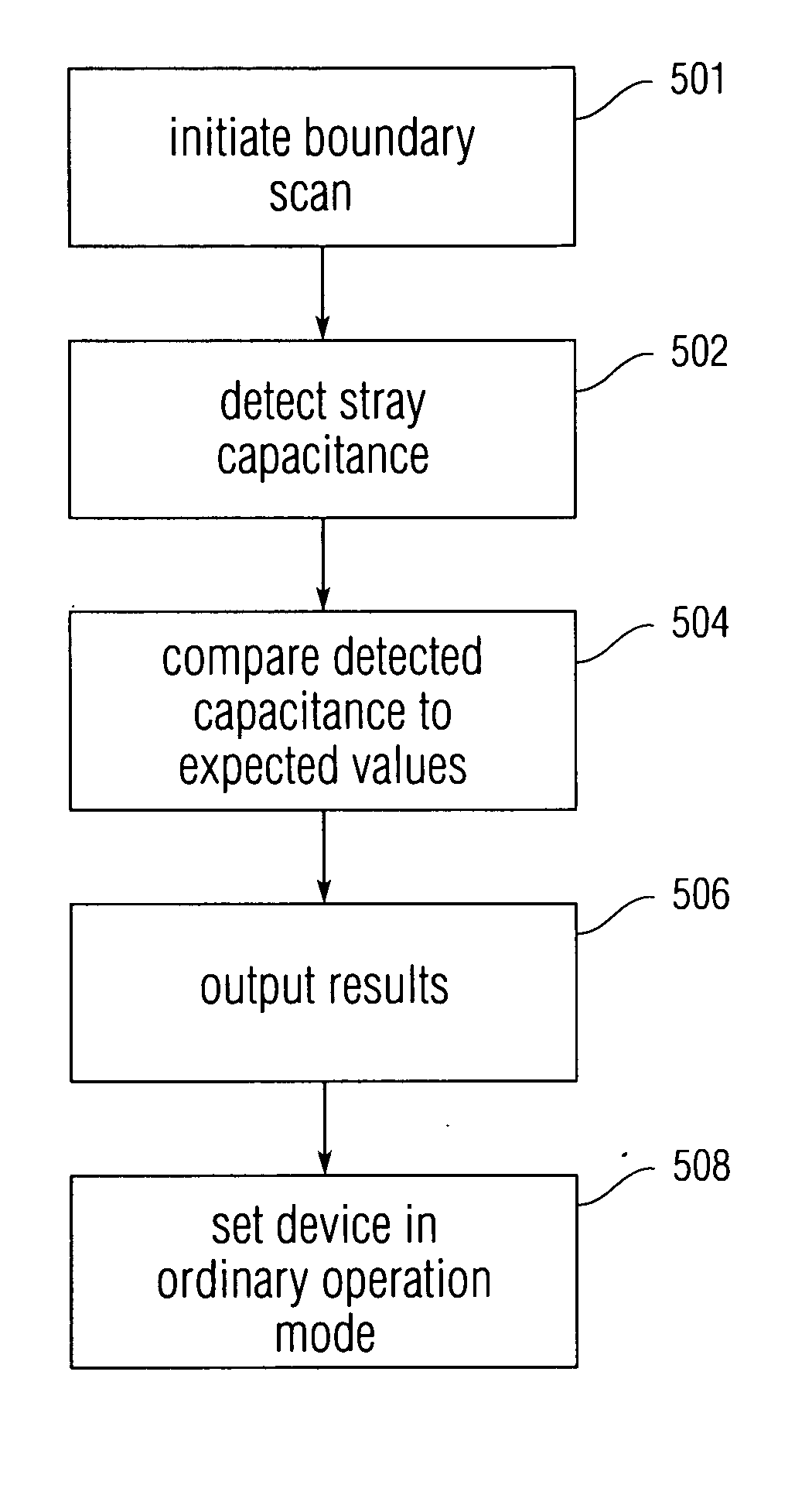
[0024]In the following description of preferred embodiments, reference is made to the accompanying drawings which form a part hereof, and in which it is shown by way of illustration specific embodiments in which the invention may be practiced. It is to be understood that other embodiments may be used and structural changes may be made without departing from the scope of the preferred embodiments of the present invention.

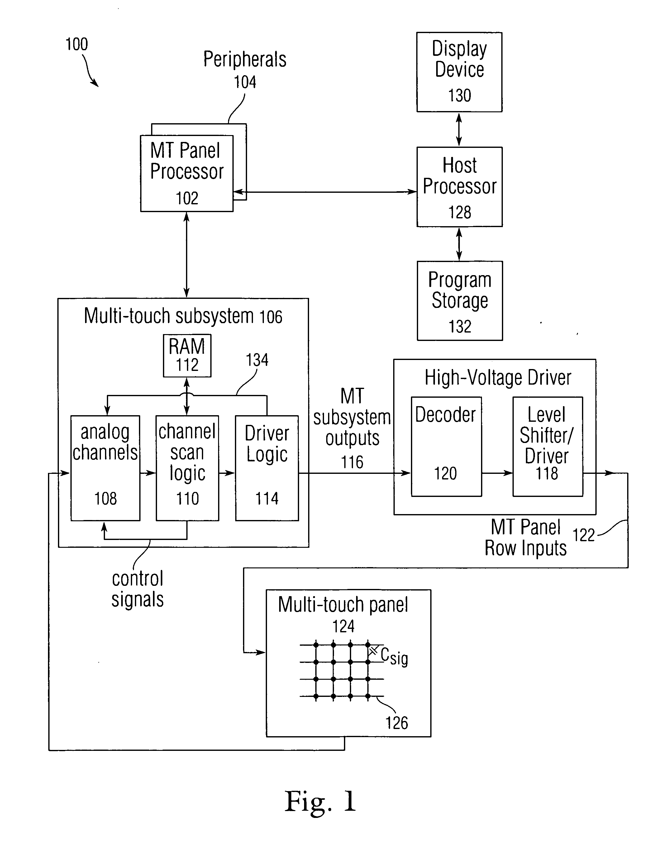
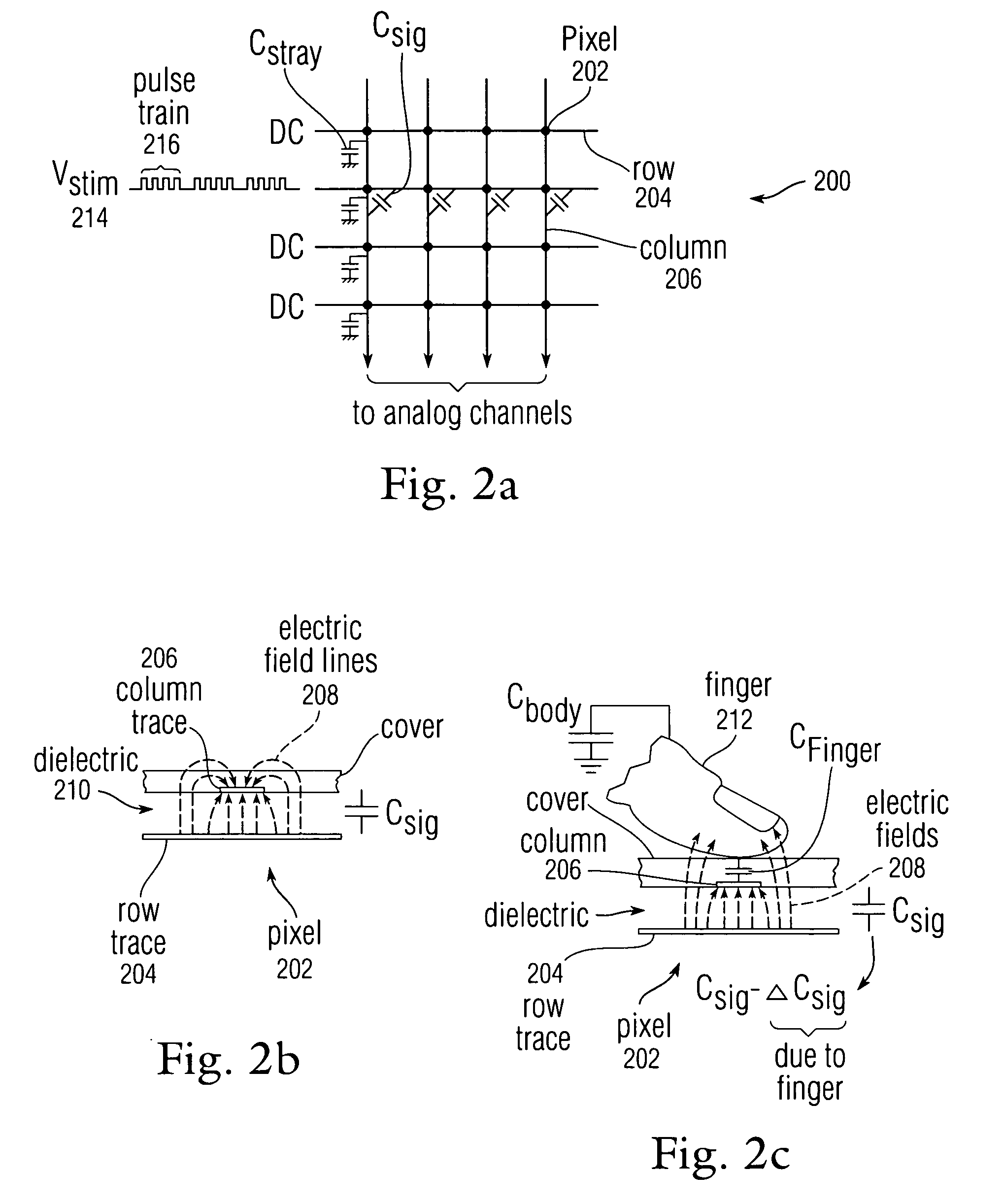
[0025]Although embodiments of the present invention are described herein in relation to an electronic device having multi-touch panel, it should be understood that the present invention is not limited to such devices, but is generally applicable to any electronic device which may benefit from boundary scanning.

[0026]The embodiments of the present invention can be used in variety of settings. One example of such a setting is an electronic device featuring a touch screen which is configured to detect multiple simultaneous touches thereon. A device including such a touc...


PUM


Abstract

Embodiments of the present invention are directed to performing boundary scanning without using a pin which is exclusively dedicated for that purpose. The boundary scan can be performed by an integrated circuit by utilizing a pin which has an alternative use during ordinary operation of the integrated circuit and the device. This pin can be connected to an analog circuit configured to sense capacitance outside of the pin. The analog circuit may also have an alternative function in normal operation of the device. During a testing mode, the analog circuit can sense a stray capacitance present at the pin. The sensed capacitance can be compared to one or more stored expected capacitance values to determine an interconnection state of the system.

Description

FIELD OF THE INVENTION[0001]This invention relates to self testing in an electronic device, and more particularly, to testing whether various modules are properly interconnected in an electronic device.BACKGROUND OF THE INVENTION[0002]When digital devices are manufactured, they are usually tested to ensure that there are no errors in manufacture. These tests may be performed immediately after manufacture and before distribution of a digital device or, in some cases, during manufacture of the digital device. Due to the advanced miniaturization of modern electronics, testing of digital devices by external monitoring is relatively difficult. That is, it is not easy to determine by external monitoring whether various components are properly functioning and / or properly connected. Therefore, many of the more complex modern electronic devices include testing circuitry as part of the device. The testing circuitry is used at the time of manufacture to perform various tests and, for some devi...

Claims


Application Information

Patent Timeline
Patent Type & Authority Applications(United States)
IPC IPC(8): G01R31/04
CPCG01R31/2815G01R31/046G01R31/70
Inventor KRAH, CHRISTOPH HORST
Owner APPLE INC
Why Eureka
Try Eureka