

Semiconductor package having a semiconductor chip in a substrate and method of fabricating the same
a semiconductor chip and semiconductor technology, applied in the direction of semiconductor devices, semiconductor/solid-state device details, electrical equipment, etc., can solve the problems of warping of the semiconductor chip having a relatively thin thickness, defects in and the relatively thin thickness of the semiconductor chip. to achieve the effect of improving the reliability of the solder ball join
- Summary
- Abstract
- Description
- Claims
- Application Information
AI Technical Summary
Benefits of technology
Problems solved by technology
Method used
Image

Examples
Embodiment Construction
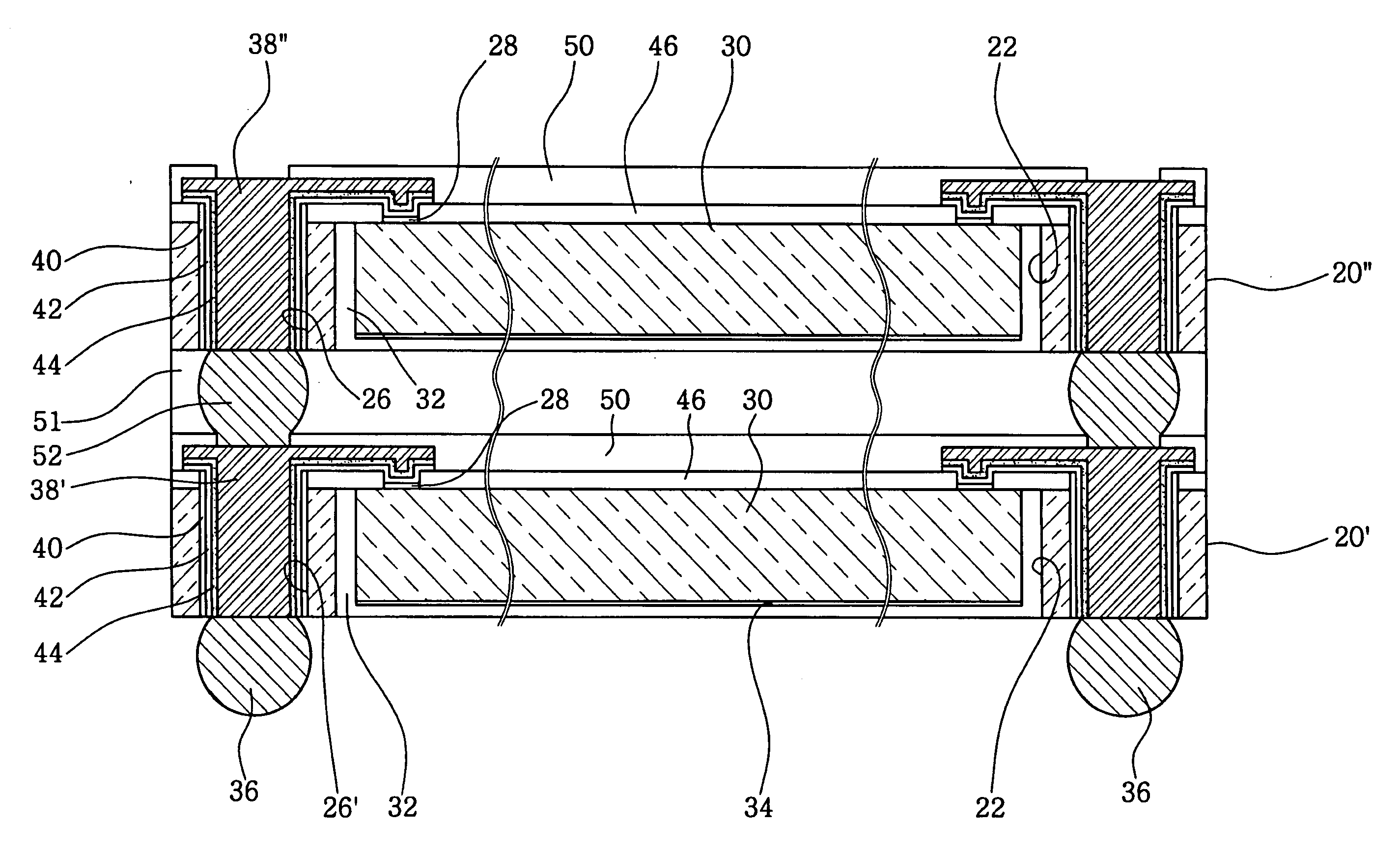
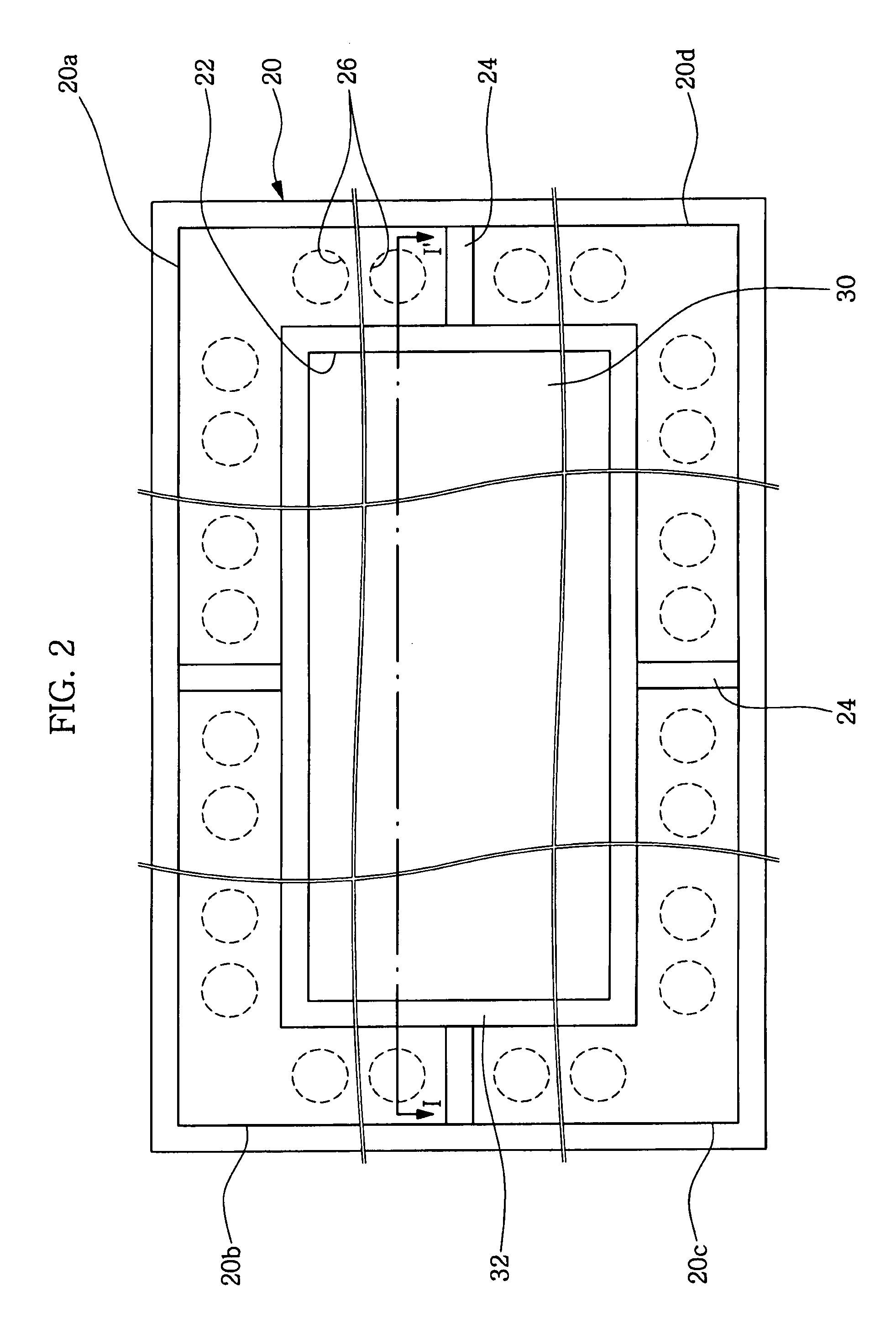
[0006]Example embodiments provide a semiconductor package that may improve solder ball joint reliability. The semiconductor package may include a semiconductor substrate having a first through hole and a plurality of second through holes spaced apart from the first through hole. The second through holes may surround the first through hole. A semiconductor chip having a plurality of pads may be disposed in the first through hole. Solder balls electrically connected to the pads may be attached to end portions of the second through holes.
[0007]The semiconductor package may include conductive layers covering the sidewalls of the second through holes and electrically connected to the pads and the solder balls. The semiconductor package may further include redistribution traces connecting the conductive layers to the pads. Alternatively, the semiconductor package may include bonding wires connecting the conductive layers to the pads. The semiconductor package may include conductive vias f...
PUM
 Abstract
Description
Claims
Application Information