

Electronic control apparatus and method of manufacturing the same
- Summary
- Abstract
- Description
- Claims
- Application Information
AI Technical Summary
Benefits of technology
Problems solved by technology
Method used
Image

Examples
first embodiment
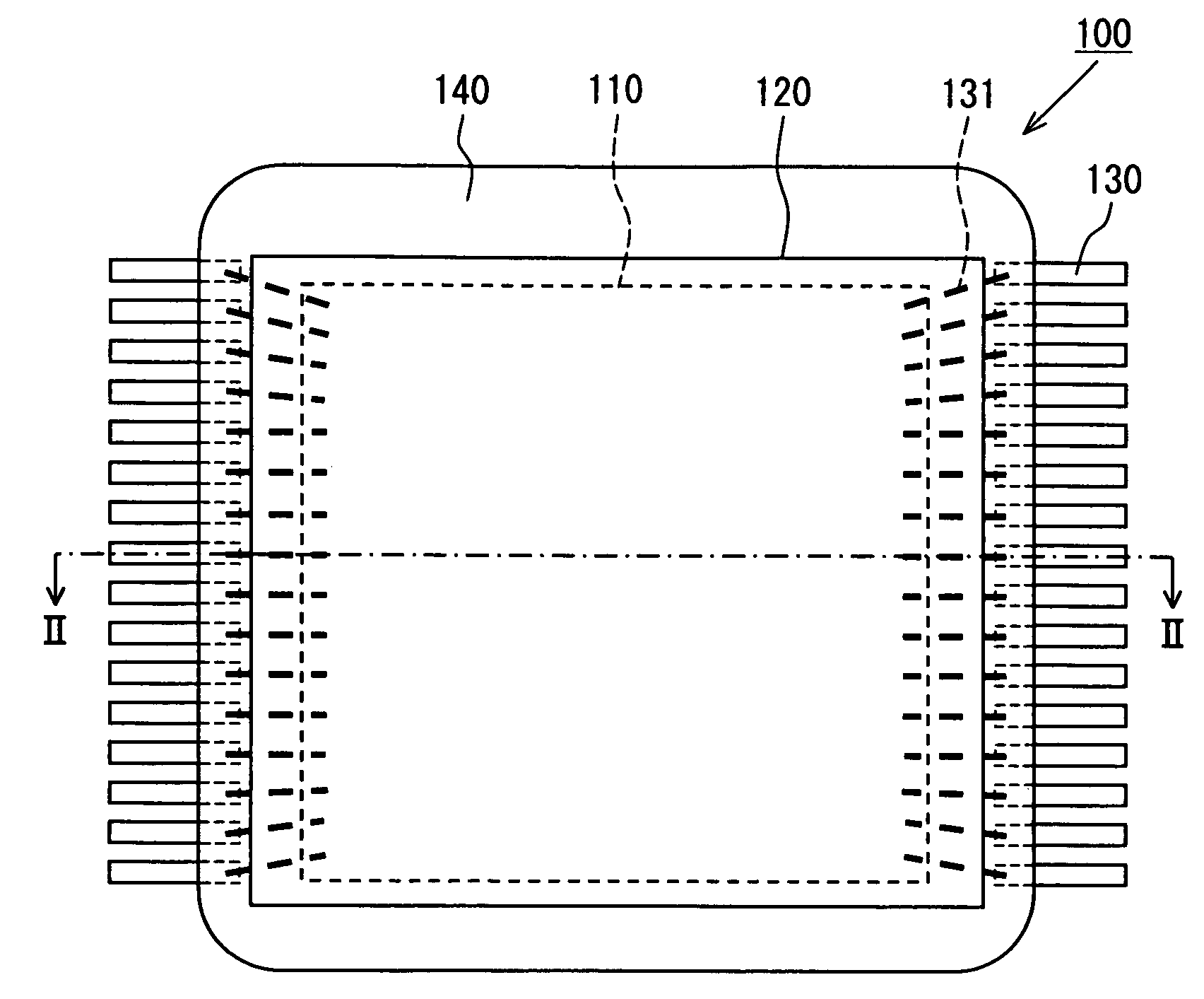
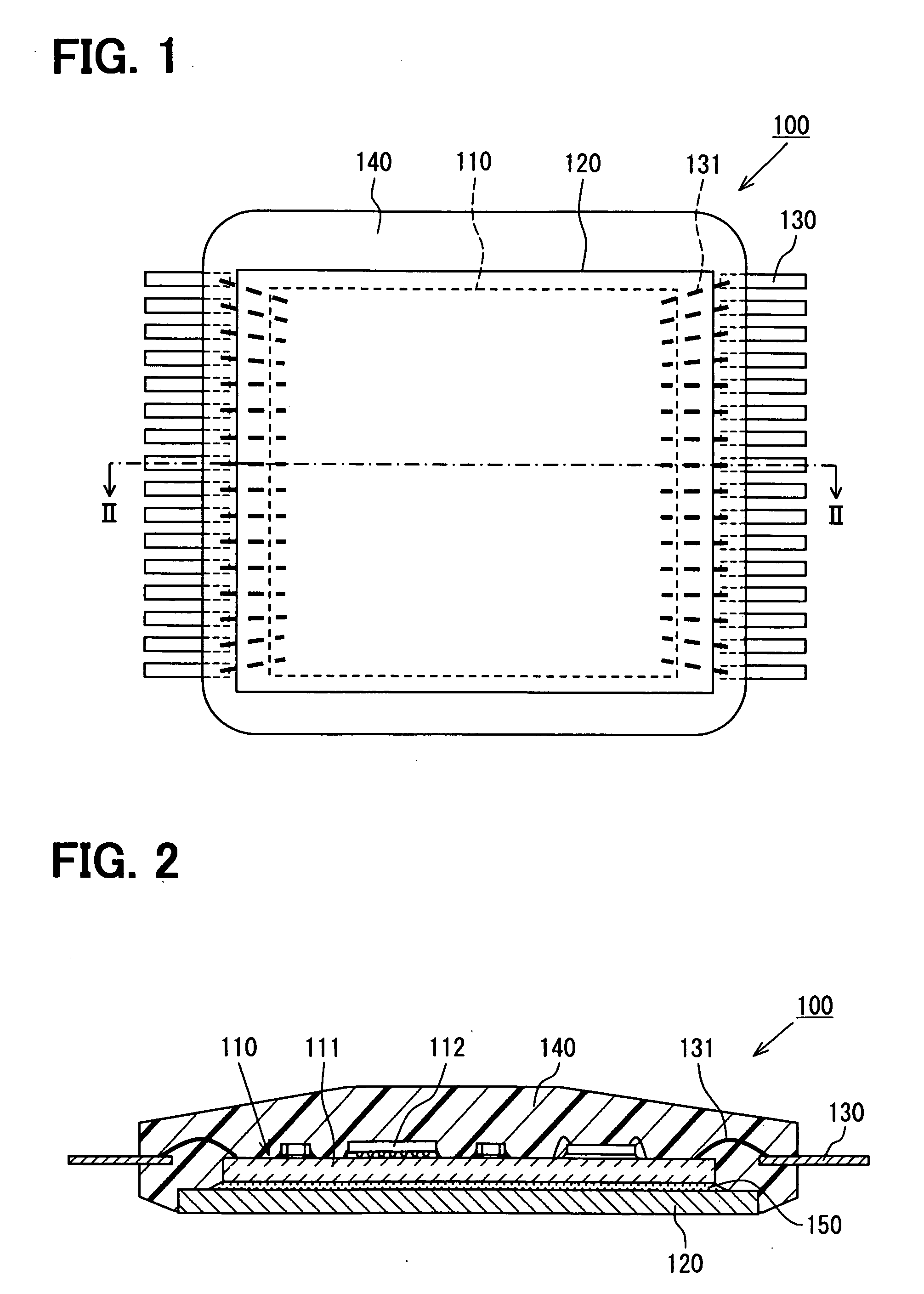
[0019]Referring to FIGS. 1, 2, an electronic control apparatus 100 according to a first embodiment of the present invention includes a circuit board 110, a heatsink 120 having a front surface on which the circuit board 110 is mounted, a lead terminal 130 having a first end electrically connected to the circuit board 110, an molding resin 140 for covering the circuit board 110 and the first end of the lead terminal 130. The molding resin 140 is placed on the circuit board 110 in such a manner that the heatsink 120 and the lead terminal 130 are partially exposed outside the molding resin 140. Specifically, as shown in FIG. 2, a back surface of the heatsink 120 and a second end of the lead terminal 130 are exposed from the molding resin 140. For example, the electronic control apparatus 100 may be installed on a vehicle. Specifically, the electronic control apparatus 100 may be used for a automatic transmission. In this case, the electronic control apparatus 100 may be combined with co...
second embodiment
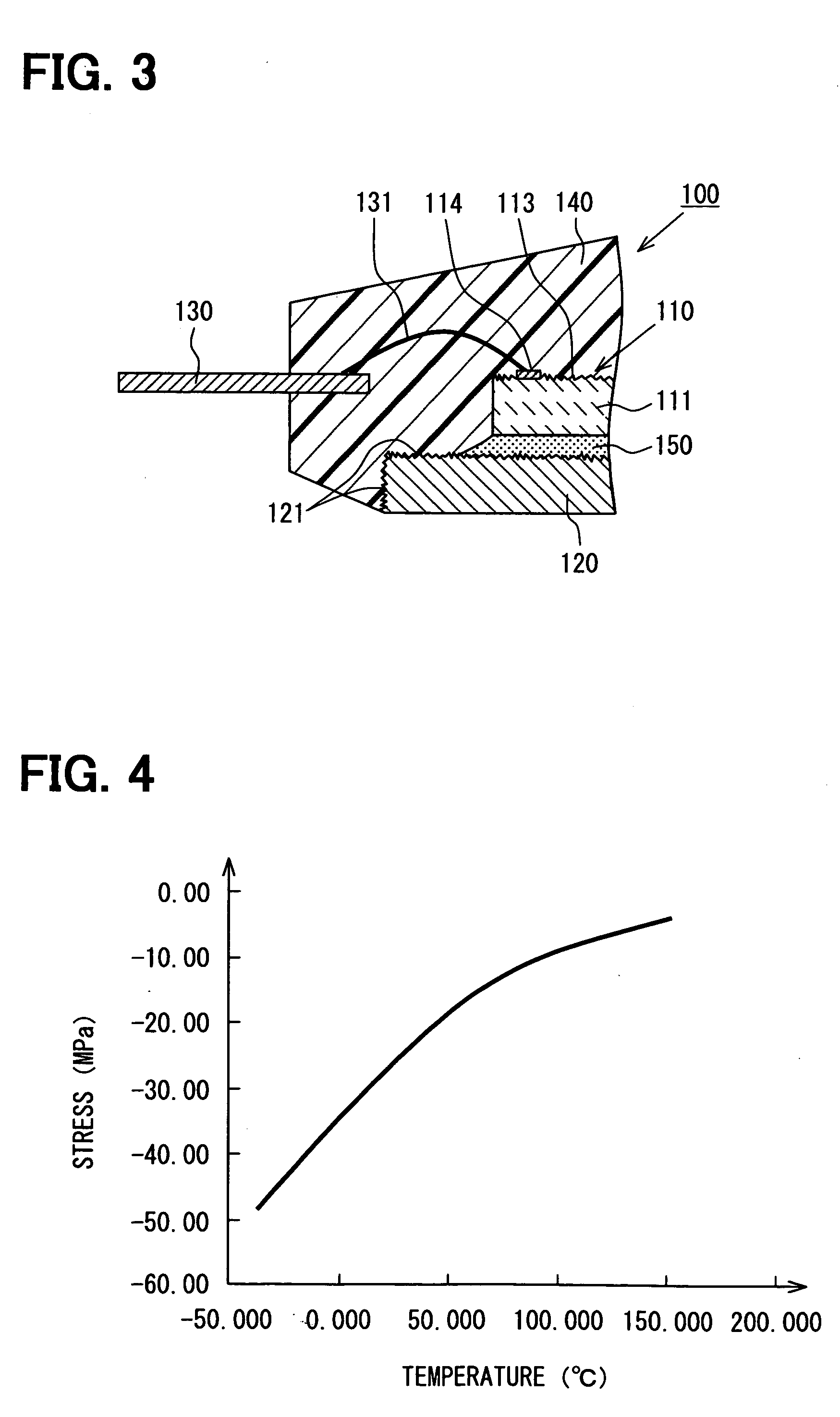
[0056]An electronic control apparatus 200 according to a second embodiment of the present invention is described below with reference to FIG. 8. Differences between the electronic control apparatus 100, 200 are as follows.
[0057]In the electronic control apparatus 100, the roughened surfaces (i.e., uneven portions 113, 121) of the circuit board 110 and the heatsink 120 directly contact the molding resin 140. In contrast, in the electronic control apparatus 200, the roughened surfaces of the circuit board 110 and the heatsink 120 contact the molding resin 140 through a coupling layer 160 that increases an adhesion of the molding resin 140 to the roughened surfaces of the circuit board 110 and the heatsink 120.
[0058]For example, the coupling layer 160 can be formed with a coupling material that has an elasticity less than that of each of the circuit board 110, the heatsink 120, and the molding resin 140, or a coupling material that makes a chemical bond with the circuit board 110, the ...
PUM
| Property | Measurement | Unit |
|---|---|---|
| Polarity | aaaaa | aaaaa |
| Adhesion strength | aaaaa | aaaaa |
| Moldable | aaaaa | aaaaa |
Abstract
Description
Claims
Application Information