Multi-chip Packaged LED Light Source
- Summary
- Abstract
- Description
- Claims
- Application Information
AI Technical Summary
Benefits of technology
Problems solved by technology
Method used
Image

Examples
Embodiment Construction
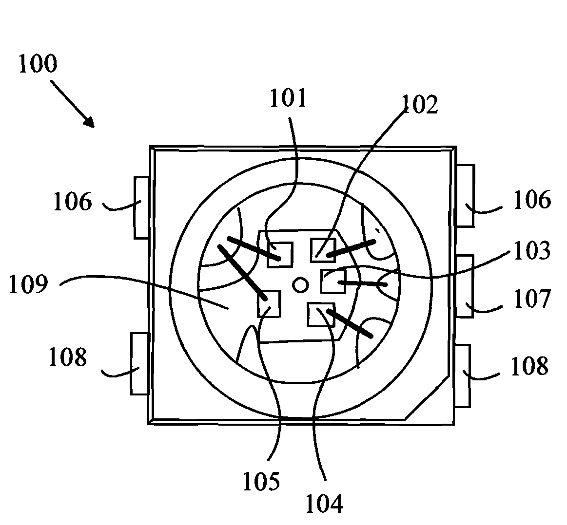
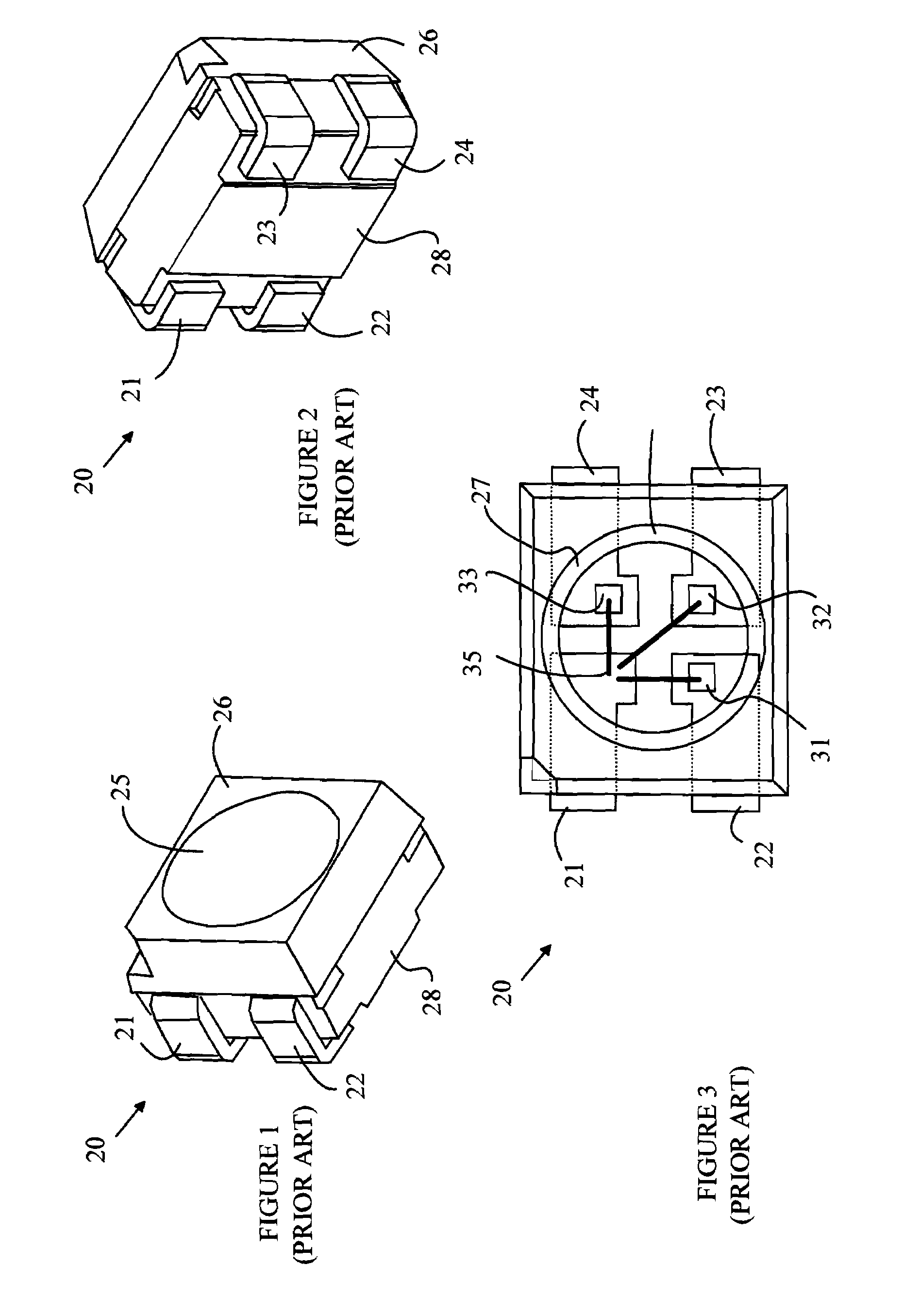
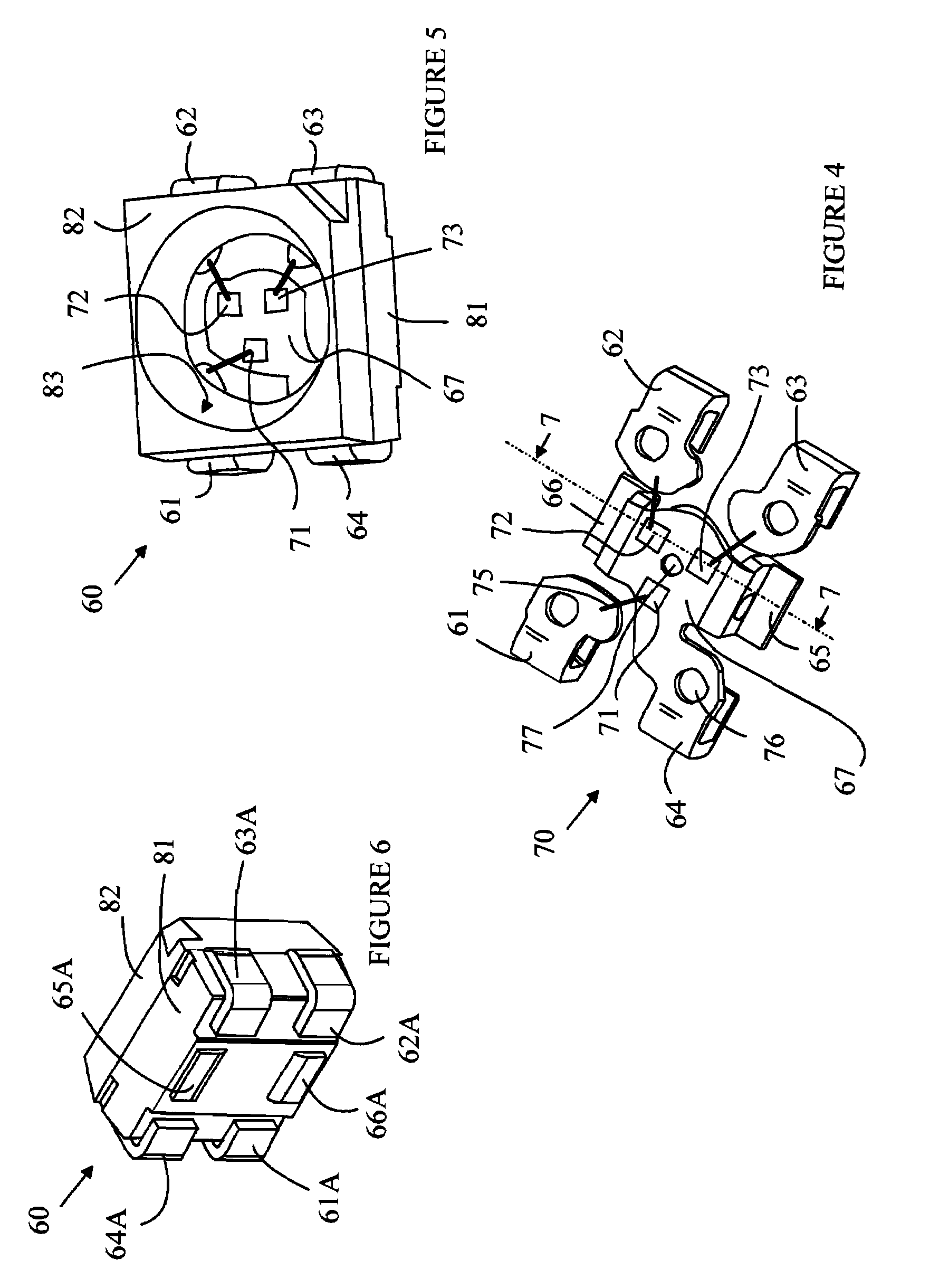
[0015]The manner in which the present invention provides its advantages can be more easily understood with reference to FIGS. 1-3, which illustrate a prior art multi-LED packaged light source 20. FIGS. 1 and 2 are perspective views of light source 20, and FIG. 3 is a top view of light source 20. To simplify the drawings, the details of the die placements and connections have been omitted from FIG. 1.
[0016]Light source 20 is constructed from a lead frame that is cut to provide leads 21-24 in the finished light source. LED dies 31-33 are mounted on leads 22-24, respectively. The dies are powered by applying a potential to a first contact on the bottom of each LED and a second contact on the top of each LED. The second contacts are connected to lead 21 by wire bonds such as wire bond 35. The contacts are accessed by the portion of the leads that extend outside the package.
[0017]The package includes two parts. The lower part 28 is molded around the leads after the dies have been attache...
PUM
 Abstract
Description
Claims
Application Information
 - Generate Ideas
- Intellectual Property
- Life Sciences
- Materials
- Tech Scout
- Unparalleled Data Quality
- Higher Quality Content
- 60% Fewer Hallucinations
Browse by: Latest US Patents, China's latest patents, Technical Efficacy Thesaurus, Application Domain, Technology Topic, Popular Technical Reports.
© 2025 PatSnap. All rights reserved.Legal|Privacy policy|Modern Slavery Act Transparency Statement|Sitemap|About US| Contact US: help@patsnap.com