Memory controller connectivity

a memory controller and connectivity technology, applied in the field of memory controllers, can solve the problems of inefficiency of wide memory controllers, increase the pin count of memory controllers, and single use, and achieve the effects of avoiding erroneous read and write operations, reducing the number of pins, and increasing bandwidth memory

Active Publication Date: 2008-07-17
ARM LTD
View PDF5 Cites 22 Cited by
  • Summary
  • Abstract
  • Description
  • Claims
  • Application Information

AI Technical Summary

Benefits of technology

[0010]In this way, an increased bandwidth memory controller can be provided which is efficient for both short and long burst lengths and which has interface circuitry with a relatively low pin count. The present technique recognises that memory devices which can be operated in a burst mode, whereby a single command provided on the address and control bus is used to transfer multiple items of data on subsequent clock edges, utilise the address and control bus less than the data bus. As a result, when a memory controller is to control the communication of data to and from a plurality of memory devices, a

Problems solved by technology

However, the use of a single, wide memory controller is inefficient unless data is being transferred in long (i.e. wide) bursts, and the use of mu

Method used


Image

  • Memory controller connectivity
  • Memory controller connectivity
  • Memory controller connectivity

Examples


Embodiment Construction

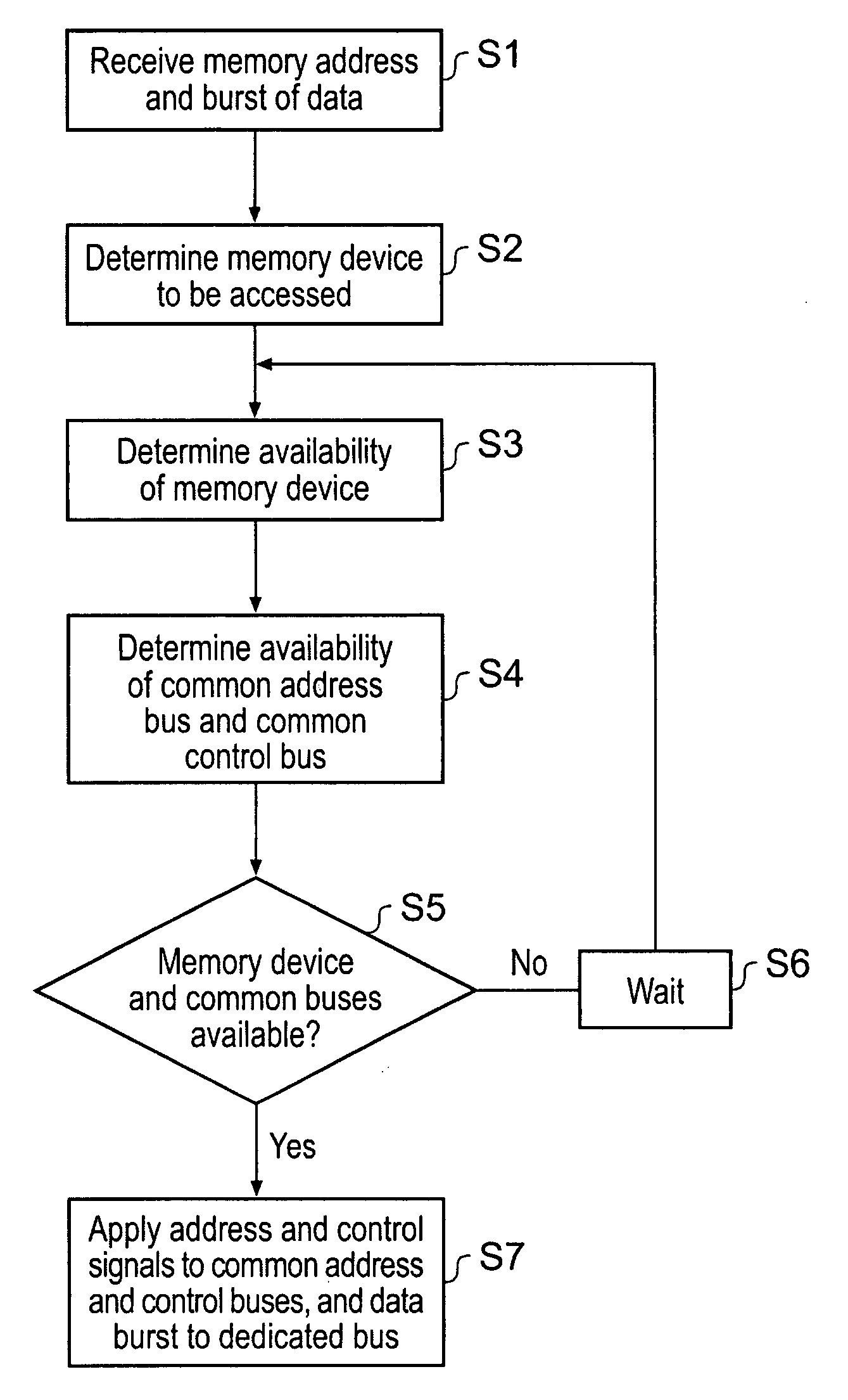
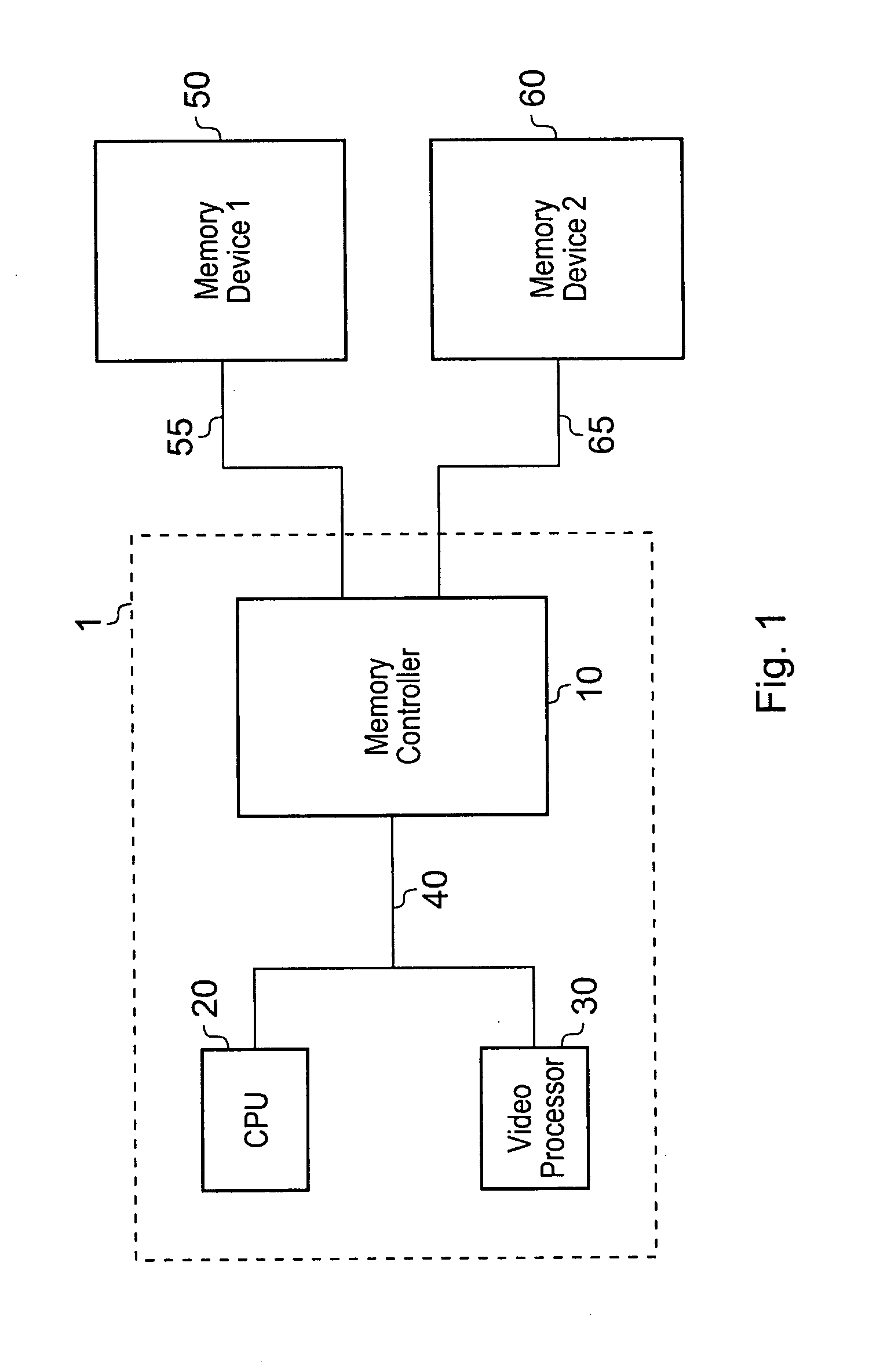
[0035]In FIG. 1, a data processing apparatus 1 includes a CPU 20, a video processor 30 and a memory controller 10 which are connected together by a bus 40. The CPU 20 and the video processor 30 are each operable to write data to or read data from an external memory device connected to the data processing apparatus 1. In particular, a first memory device 50 (memory device 1) is connected to the memory controller 10 via a bus 55, and a second memory device 60 (memory device 2) is connected to the memory controller 10 via a bus 65. The CPU 20 or the video processor 30 are each operable to read data from one or other (or both) of the memory devices 50, 60 by applying an address signal indicating the physical location of the desired data on a memory device to the memory controller 10 on the bus 40. The memory controller 10 is responsive to the applied address, control signal to provide address and control signals to the appropriate memory device to control a transfer of data from the mem...


PUM


Abstract

A memory controller with an interface for providing a connection to a plurality of memory devices at least one of said plurality of memory devices supporting burst mode data transfers comprises data interface circuitry for connecting to a plurality of separate data buses for communicating data signals between said memory controller and a respective one of said memory devices, each of said data buses providing a dedicated data signal path to a different one of said memory devices, address interface circuitry for connecting to a common address bus for communicating address signals to each of said memory devices on a shared address signal path, address signals which are directed to different ones of said memory devices being time division multiplexed together on said common address bus, and device selecting circuitry for generating one or more device selecting signals synchronised with said time division multiplexing of said common address bus to select that memory device to which address signals currently asserted on said common address bus are directed. In this way, an increased bandwidth memory controller can be provided which is efficient for both short, narrow and long and wide burst lengths and which has interface circuitry with a relatively low pin count.

Description

BACKGROUND OF THE INVENTION[0001]1. Field of the Invention[0002]This invention relates to memory controllers. More particularly, this invention relates to memory controllers for providing a connection to a plurality of memory devices.[0003]2. Description of the Prior Art[0004]A memory controller may be provided within a data processing apparatus to provide an interface between memory addressing components of the data processing apparatus, such as a central processing unit (CPU) or a co-processor, and an external memory device which is addressable by those components. A large number of input / output (I / O) pins are usually required to provide a suitable communications interface between the memory controller and the memory device. The input / output pins can be generally grouped into a data bus for communicating data signals, which represent information content to be stored or read, an address bus for communicating address signals, which represent the location within the memory device whe...

Claims


Application Information

Patent Timeline
IPC IPC(8): G06F12/06G06F13/00G06F13/10
CPCG06F13/1684
Inventor CROXFORD, DAREN
Owner ARM LTD
Why Eureka
Try Eureka