

Novel magnetic tunnel junction (MTJ) to reduce spin transfer magnetization switching current
a technology of magnetic tunnel junction and switching current, which is applied in the direction of magnetic field-controlled resistors, galvano-magnetic devices, semiconductor devices, etc., can solve the problems of no prior art references, diffuse into nife, and the resistance of the transistor connected to the mtj is too high, so as to reduce the magnetic “dead layer”
Active Publication Date: 2008-07-31
TAIWAN SEMICON MFG CO LTD
View PDF10 Cites 177 Cited by
- Summary
- Abstract
- Description
- Claims
- Application Information
AI Technical Summary
Benefits of technology
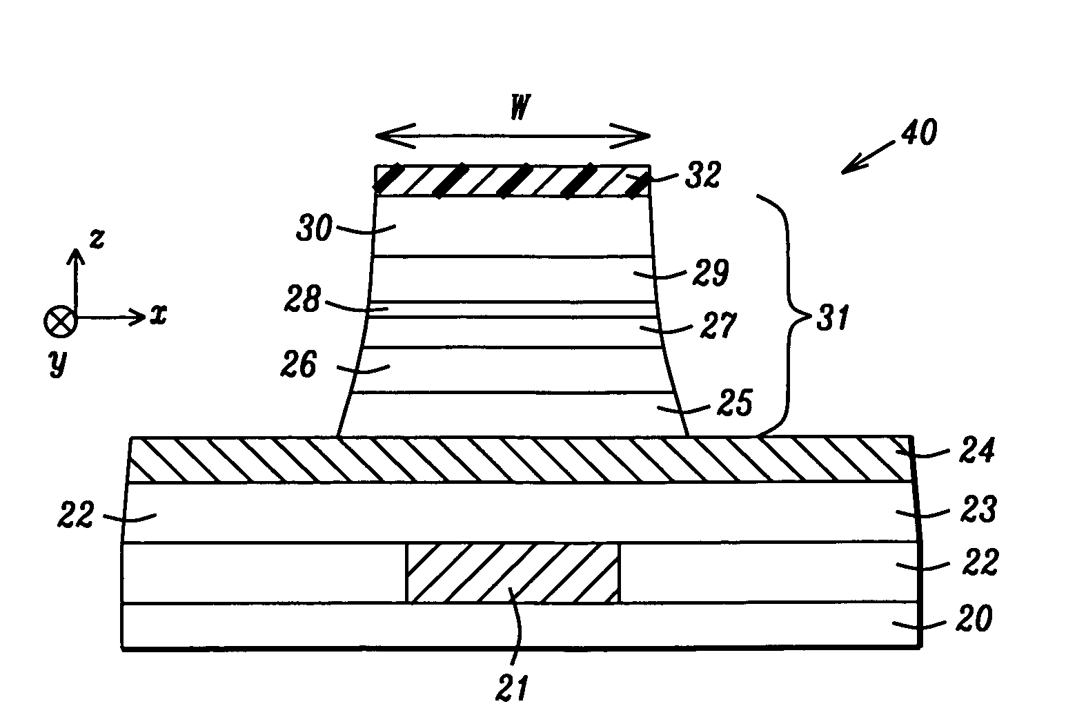
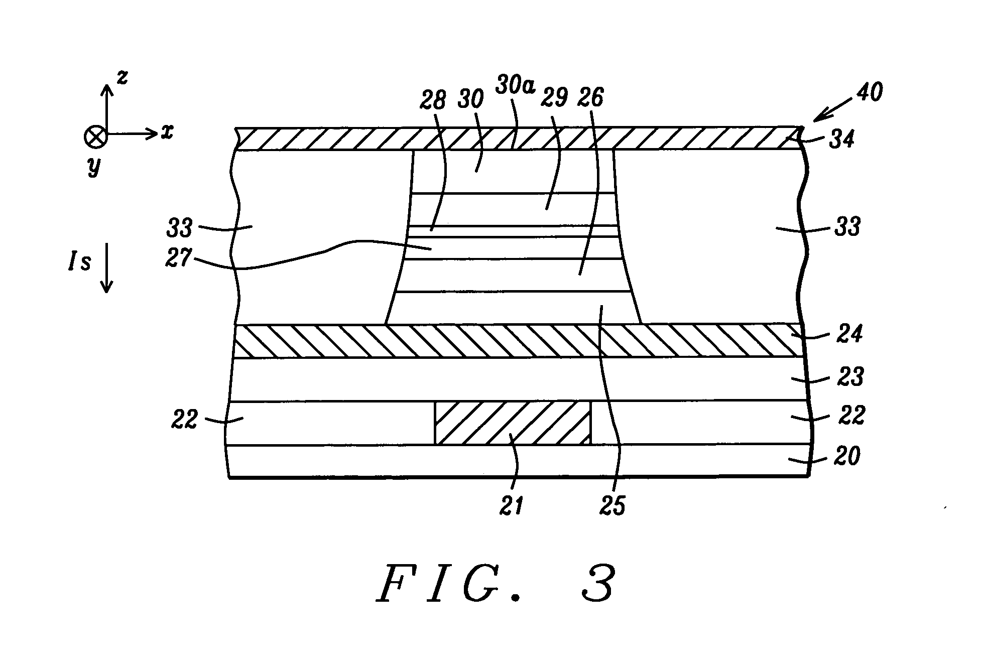
[0023]According to a first embodiment, these objectives are achieved by providing a substrate comprised of a bottom conductor electrode on which a Spin-RAM structure is to be fabricated. An MTJ element is formed by first depositing a stack of layers on the bottom conductor electrode. In one aspect, the MTJ stack has a bottom spin valve configuration in which a seed layer, AFM layer, synthetic anti-ferromagnetic (SyAF) pinned layer, tunnel barrier layer, free layer, and a capping layer are sequentially formed. Preferably, the pinned layer has a synthetic anti-ferromagnetic (SyAF) configuration wherein a Ru coupling layer is sandwiched between a lower CoFe (AP2) layer and an upper amorphous CoFeB (AP1) layer. The tunnel barrier layer may be comprised of crystalline MgO. Above the tunnel barrier layer is a free layer comprised of amorphous CoFeB. A Hf/Ru capping layer may be employed on the free layer. The lower layer in the capping layer is preferably Hf in order
Problems solved by technology
Otherwise, R would be too high to match the resistance of the transistor which is connected to the MTJ.
The disadvantage of using a Ta capping layer is that Ta diffuses into NiFe during thermal annealing, especially at high annealing temperatures (i.e. >250° C.) to produce an alloy that not only reduces free layer moment (Bs) but makes NiFe very magnetostrictive with a λs of ≧5×10⁻⁶.
However, to our knowledge, non
Method used
View moreImage
Smart ImageViewing Examples

Examples
 PUM
 Abstract
A MTJ that minimizes spin-transfer magnetization switching current (Jc) in a Spin-RAM to <1×10⁶ A/cm2 is disclosed. The MTJ has a Co60Fe20B20/MgO/Co60Fe20B20 configuration where the CoFeB AP1 pinned and free layers are amorphous and the crystalline MgO tunnel barrier is formed by a ROX or NOX process. The capping layer preferably is a Hf/Ru composite where the lower Hf layer serves as an excellent oxygen getter material to reduce the magnetic “dead layer” at the free layer/capping layer interface and thereby increase dR/R, and lower He and Jc. The annealing temperature is lowered to about 280° C. to give a smoother CoFeB/MgO interface and a smaller offset field than with a 350° C. annealing. In a second embodiment, the AP1 layer has a CoFeB/CoFe configuration wherein the lower CoFeB layer is amorphous and the upper CoFe layer is crystalline to further improve dR/R and lower RA to ≦10 ohm/μm2.
Description
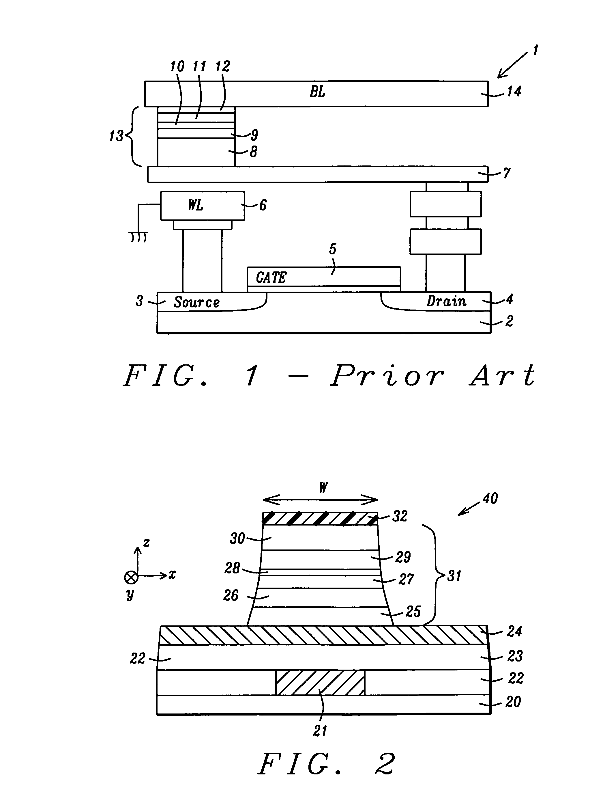
RELATED PATENT APPLICATIONS[0001]This application is related to the following: Docket # HMG06-011 / 012, Ser. No. 11 / 496,691, filing date Jul. 31, 2006; and Docket # HMG05-043, Ser. No. 11 / 317,388, filing date Dec. 22, 2005, assigned to a common assignee.FIELD OF THE INVENTION[0002]The invention relates to a high performance Magnetic Tunneling Junction (MTJ) element and a method for making the same, and more particularly, to a configuration comprised of a composite AP1 pinned layer, a MgO barrier layer, an amorphous CoFeB free layer, and a Hf capping layer that minimizes the “dead layer” at the free layer / capping layer interface and reduces spin transfer magnetization switching current in a Spin-RAM device.BACKGROUND OF THE INVENTION[0003]Magnetoresistive Random Access Memory (MRAM), based on the integration of silicon CMOS with MTJ technology, is a major emerging technology that is highly competitive with existing semiconductor memories such as SRAM, DRAM, Flash, etc. A MRAM device i...
Claims
Login to View More Application Information
Patent Timeline
 IPC IPC(8): H01L43/00
CPCH01L43/12H01L43/08H10N50/10H10N50/01
InventorHORNG, CHENG T.TONG, RU-YING
OwnerTAIWAN SEMICON MFG CO LTD