Methods and apparatus for engineering an interface between a diffusion barrier layer and a seed layer

a diffusion barrier layer and seed layer technology, applied in the direction of vacuum evaporation coating, semiconductor/solid-state device details, coatings, etc., can solve the problems of unfavorable non-conform deposition of large amounts of seed layer material, formation of voids during electroplating, and formation of unacceptably large overhangs at feature openings. , to achieve the effect of improving stress and electromigration resistance, improving adhesion to the underlying barrier layer, and high stability

Inactive Publication Date: 2010-12-21
NOVELLUS SYSTEMS
View PDF199 Cites 37 Cited by
  • Summary
  • Abstract
  • Description
  • Claims
  • Application Information

AI Technical Summary

Benefits of technology

[0006]As the dimensions of features in integrated circuits (IC) scale down, non-conformal deposition of large amounts of seed layer material becomes less feasible. In narrow recessed features (e.g., in features having widths of about 65 nm and less, and particularly in features having widths of about 45 nm and less), deposition of large amounts of seed layer material can lead to formation of unacceptably large overhangs at the feature openings. The overhangs may partially or completely close the features to deposition of additional material, thereby leading to formati

Problems solved by technology

As the dimensions of features in integrated circuits (IC) scale down, non-conformal deposition of large amounts of seed layer material becomes less feasible.
In narrow recessed features (e.g., in features having widths of about 65 nm and less, and particularly in features having widths of about 45 nm and less), deposition of large amou

Method used


Image

  • Methods and apparatus for engineering an interface between a diffusion barrier layer and a seed layer
  • Methods and apparatus for engineering an interface between a diffusion barrier layer and a seed layer
  • Methods and apparatus for engineering an interface between a diffusion barrier layer and a seed layer

Examples


Embodiment Construction

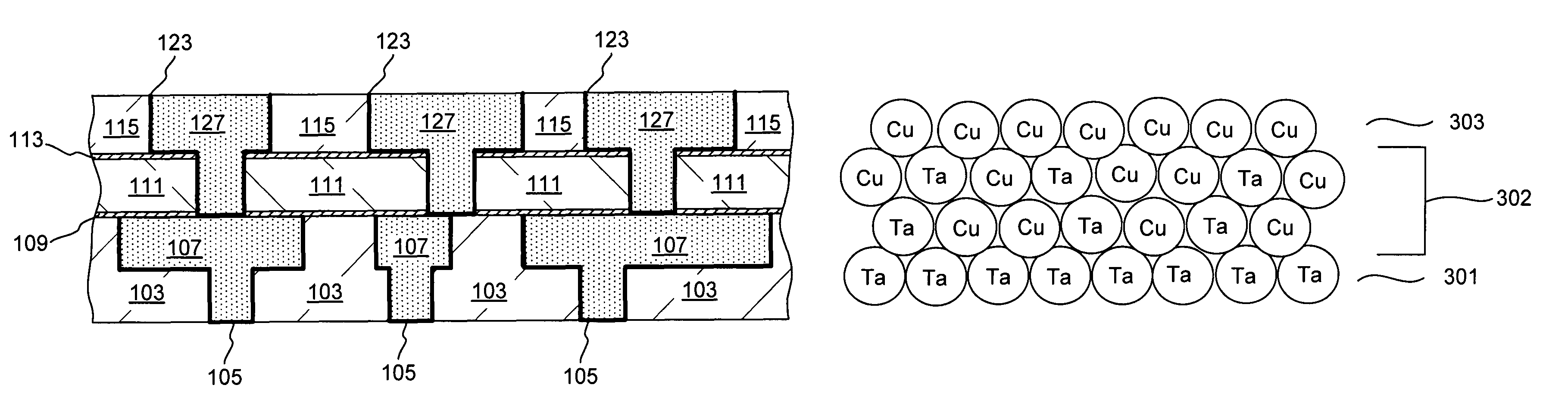
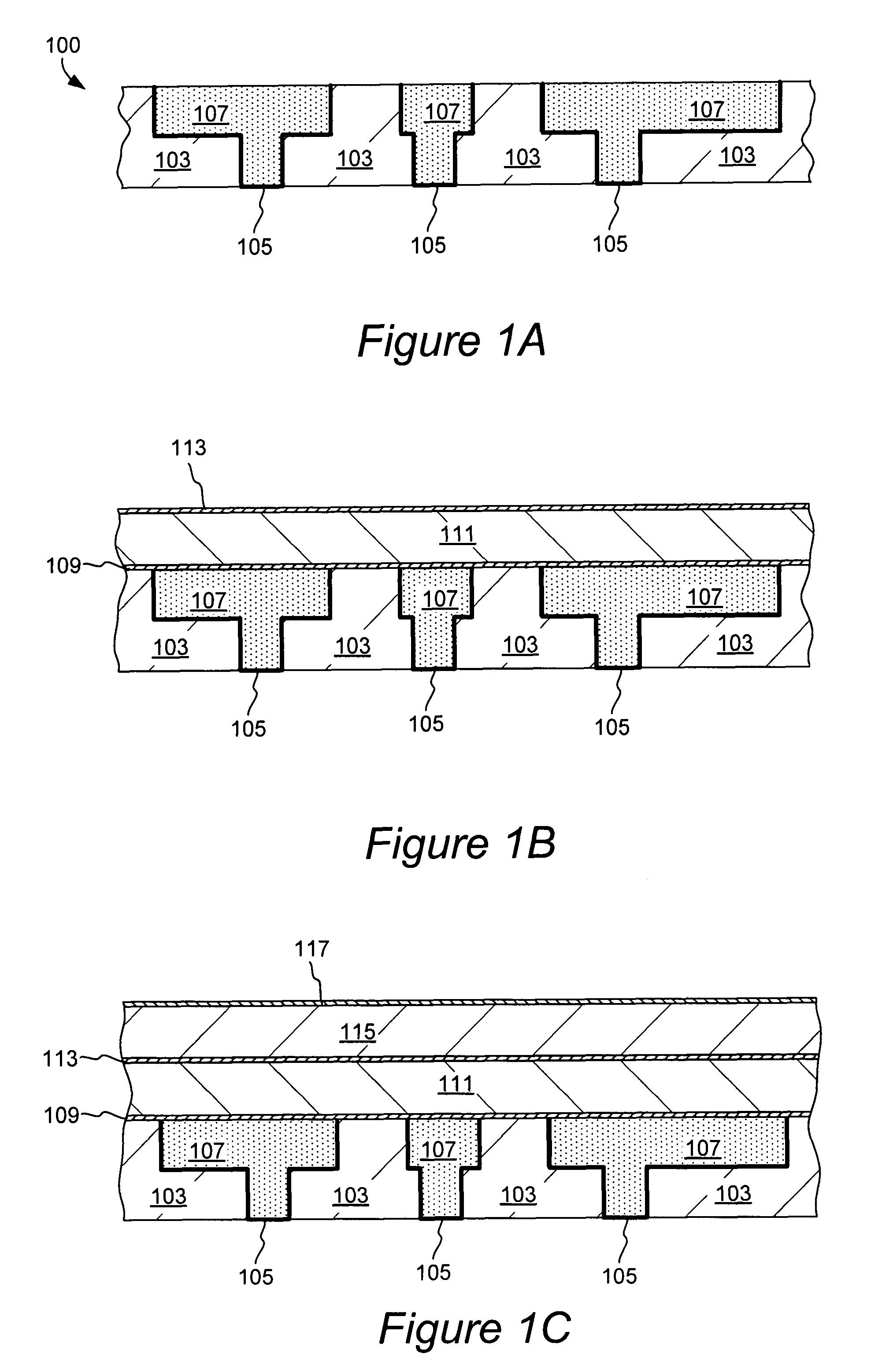
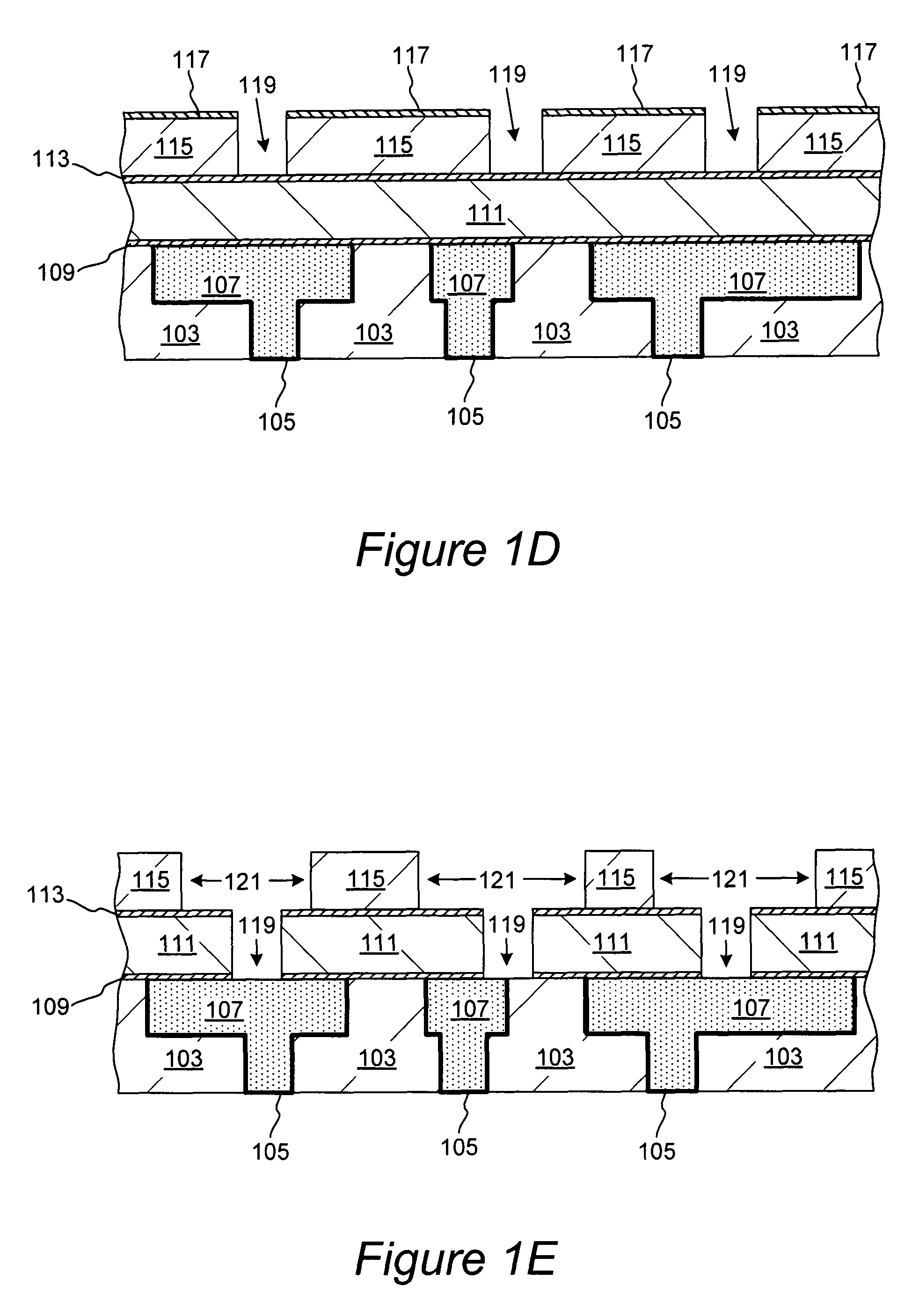
[0038]Thin and continuous copper seed layers can be formed on top of tantalum-containing diffusion barrier layers when agglomeration of copper is prevented with the use of an engineered interface between the two layers. The engineered interface includes an adhesion layer in which copper atoms are physically trapped such that they cannot easily migrate and agglomerate. The trapped copper atoms serve as the nucleation sites for the subsequently deposited copper-containing material.

[0039]Copper seed layer materials as used herein include copper and its alloys, such as CuAl, CuZn, CuMg, CuSn, CuMn, CuAg, CuB, and the like. Tantalum-containing diffusion barrier materials include, but are not limited to Ta, TaNx, TaSixNy, TaCxNy, and combinations thereof. In general, provided methods are particularly suitable for engineering an interface between materials which do not have strong chemical affinity towards each other. For example, in the case of copper and tantalum, affinity of copper to c...


PUM

PropertyMeasurementUnit
Fractionaaaaaaaaaa
Fractionaaaaaaaaaa
Fractionaaaaaaaaaa

Abstract

Copper seed layers are formed on diffusion barrier layers (e.g., on Ta, and TaNx layers) without significant agglomeration of copper, with the use of an engineered barrier layer/seed layer interface. The engineered interface includes an adhesion layer, in which copper atoms are physically trapped and are prevented from migrating and agglomerating. The adhesion layer can include between about 20-80% atomic of copper. The copper atoms of the adhesion layer are exposed during deposition of a copper seed layer and serve as the nucleation sites for the deposited copper. Thin, continuous, and conformal seed layers can be deposited on top of the adhesion layer. The trapping of copper within the adhesion layer is achieved by intermixing diffusion barrier and seed layer materials using PVD and/or ALD.

Description

CROSS-REFERENCE TO RELATED APPLICATIONS[0001]This application is a continuation-in-part claiming priority under 35 USC 120 from U.S. patent application Ser. No. 11 / 473,618 filed Jun. 22, 2006 now U.S. Pat. No. 7,645,696, titled “Deposition of Thin Continuous PVD Seed Layers Having Improved Adhesion to the Barrier Layer”, naming Dulkin et al. as inventors, which is herein incorporated by reference in its entirety for all purposes.FIELD OF THE INVENTION[0002]The present invention pertains to methods for forming a metal seed layer on a barrier layer of a partially fabricated integrated circuit.BACKGROUND OF THE INVENTION[0003]Damascene processing is a method for forming interconnections on integrated circuits that involves formation of inlaid metal lines in trenches and vias formed in a dielectric layer (inter-metal dielectric). The metal conductive lines are formed by an electroplating process. Because copper or other mobile conductive material provides the conductive paths of the int...

Claims


Application Information

Patent Timeline
IPC IPC(8): H01L21/44
CPCC23C14/022C23C14/046H01L21/02068H01L21/2855H01L21/28562H01L21/32131H01L21/76805H01L21/76813H01L21/76844H01L21/76846H01L21/76862H01L21/76865H01L21/76868H01L21/76873H01L23/53238H01L2924/0002H01L2924/00
Inventor DULKIN, ALEXANDERRAIRKAR, ASITGREER, FRANKPRADHAN, ANSHU A.ROZBICKI, ROBERT
Owner NOVELLUS SYSTEMS
Why Eureka
Try Eureka