Semiconductor device

a technology of semiconductor devices and conductors, applied in semiconductor devices, semiconductor/solid-state device details, electrical apparatus, etc., can solve the problems of increasing the complexity of the shape of the first dummy conductor pattern, the inability to transmit electrical signals, and the increase in the complexity of the shape of the dummy conductor pattern, so as to improve the stability of the transmission characteristics of wiring, the effect of inhibiting the flow of eddy curren

Active Publication Date: 2008-07-31
RENESAS ELECTRONICS CORP
View PDF4 Cites 9 Cited by
  • Summary
  • Abstract
  • Description
  • Claims
  • Application Information

AI Technical Summary

Benefits of technology

[0011]In the semiconductor device, each of the dummy conductor patterns arranged around the interconnection conductor has a polygonal shape with at least one dent which is provided at a part of a periphery of the polygonal shape. The presence of dent which is provided at a part of a periphery of the polygonal shape leads to an increase in complexity of the shape of the dummy conductor pattern. In a case where a signal flowing through the interconnection conductor is a high-frequency signal, due to the skin effect, the current density thereof is increased as the current density comes closer to the surface of the conductor. Accordingly, the complexity of the outer shape of the first dummy conductor pattern effectively inhibits the flow of the eddy current in the pattern. As a result, the eddy current decreases in magnitude, whereby the fluctuation of the circuit constant of the inductor can be suppressed to a small level.
[0012]According to the present invention, there can be achieved a semiconductor device capable of improving stability of transmission characteristics of wiring.

Problems solved by technology

Accordingly, a circuit constant of the wiring 101 fluctuates, which results in instability of transmission characteristics of the wiring 101.
The problem becomes prominent when the high-frequency current with a frequency of 5 GHz or higher flows through the wiring 101.
The presence of the internal angle leads to an increase in complexity of the shape of the first dummy conductor pattern.
The presence of dent which is provided at a part of a periphery of the polygonal shape leads to an increase in complexity of the shape of the dummy conductor pattern.

Method used


Image

  • Semiconductor device
  • Semiconductor device
  • Semiconductor device

Examples


Embodiment Construction

[0026]Hereinafter, exemplary embodiments of the present invention will be described in detail with reference to the accompanying drawings. Note that, in the description of the drawings, the same components are denoted by the same reference symbols, and redundant explanations thereof are omitted.

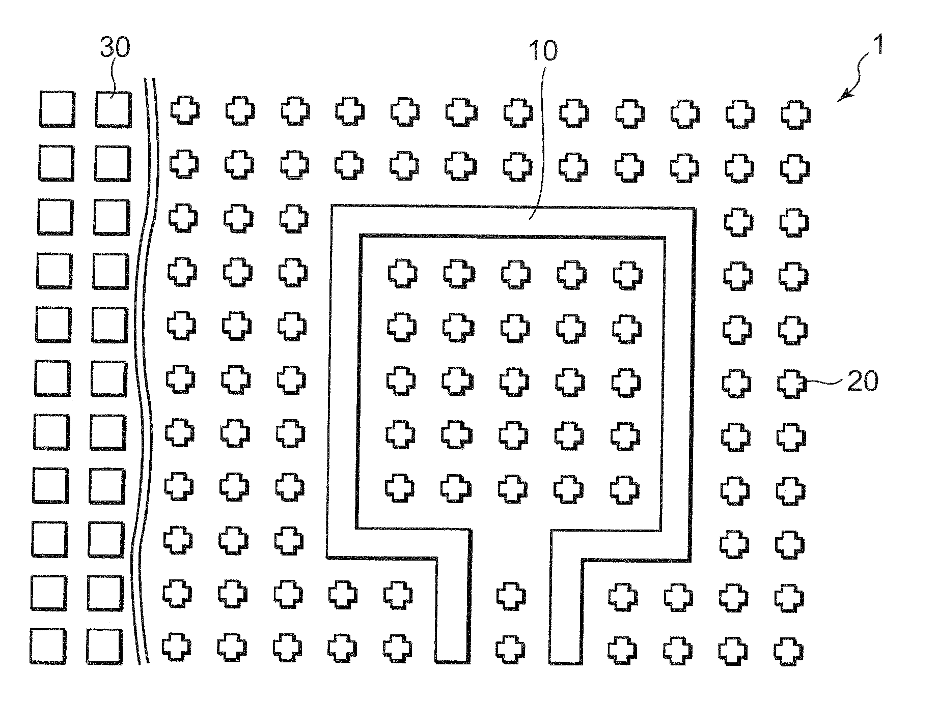
[0027]FIG. 1 is a plan view showing a semiconductor device according to an embodiment of the present invention. A semiconductor device 1 includes a wiring 10 and dummy conductor patterns 20. The wiring 10 is a wiring through which a high-frequency current with a frequency of 5 GHz or higher flows. In the embodiment of the present invention, the wiring 10 functions as an inductor.

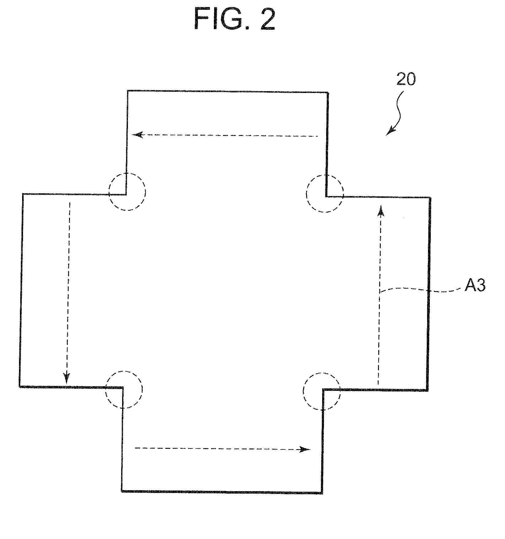
[0028]Near the wiring 10, a plurality of dummy conductor patterns 20 are formed. In this case, the dummy conductor pattern refers to a conductor pattern, presence or absence of which does not affect a circuit configuration of the semiconductor device 1. The dummy conductor patterns 20 are arranged regularly, in partic...


PUM


Abstract

A semiconductor device (1) includes a wiring (10) and dummy conductor patterns (20). The wiring (10) is a wiring through which a current with a frequency of 5 GHz or higher flows. Near the wiring (10), the dummy conductor patterns (20) are formed. A planar shape of each of the dummy conductor patterns (20) is equivalent to a shape with an internal angle larger than 180°.

Description

BACKGROUND OF THE INVENTION[0001]1. Field of the Invention[0002]The present invention relates to a semiconductor device.[0003]2. Description of the Related Art[0004]FIG. 9 is a plan view showing a semiconductor device of a related art (for example, see JP 2005-310807 A). In a semiconductor device 100, rectangular dummy conductor patterns 102 are formed near a wiring 101. The dummy conductor patterns 102 are provided so that the wiring 101 can be easily processed at the time of production of the semiconductor device 100. In addition, the wiring 101 functions as an inductor.[0005]Note that, related art documents relevant to the present invention include JP 2005-285970 A and Ali Hajimiri et al., “Design Issues in CMOS Differential LC Oscillators”, IEEE JOURNAL OF SOLID-STATE CIRCUITS, Vol. 34, No. 5, May 1999, pp. 717-724, in addition to JP 2005-310807 A.[0006]The present inventor has recognized as follows. In a case where a high-frequency current flows through the wiring 101 in the se...

Claims


Application Information

Patent Timeline
Patent Type & Authority Applications(United States)
IPC IPC(8): H01L23/48
CPCH01L23/522H01L23/5227H01L23/585H01L23/66H01L2924/0002H01L2924/00
Inventor NAKASHIBA, YASUTAKA
Owner RENESAS ELECTRONICS CORP
Why Eureka
Try Eureka