Semiconductor sensor and method of manufacturing the same

Inactive Publication Date: 2008-08-28
DENSO CORP
View PDF23 Cites 29 Cited by
  • Summary
  • Abstract
  • Description
  • Claims
  • Application Information

AI Technical Summary

Benefits of technology

[0007]In view of the above-described problem, it is an object of the present invention to provide a semiconductor s

Problems solved by technology

It is difficult to adjust a depth to which ions are implanted to form the heavily doped region.
However, it is difficult to control the diffusion in the semiconductor substrate.
The variations in the electrical resistance of the gauge section cause a reduction in detection accuracy.
The same problem can arise for other semiconductor sensors such as a semiconductor temperature sensor, which detects a volume change due to a temperature change of an object as an electrical resistance change of a gauge secti

Method used


Image

  • Semiconductor sensor and method of manufacturing the same
  • Semiconductor sensor and method of manufacturing the same
  • Semiconductor sensor and method of manufacturing the same

Examples


first embodiment

Modifications of First Embodiment

[0055]The first embodiment described above may be modified in various ways. According to the first embodiment, the stem 70 is made of a metallic material. Alternatively, the stem 70 can be made of a material than a metallic material. For example, the stem 70 can be made of a resin material such as rubber having a high elasticity. In short, the stem 70 can be made of any material that can be deformed according to a change in pressure in ambient atmosphere of the semiconductor sensor 1.

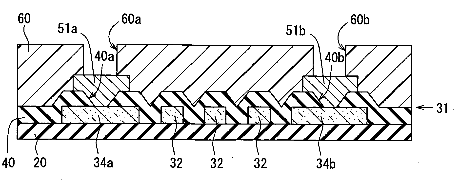
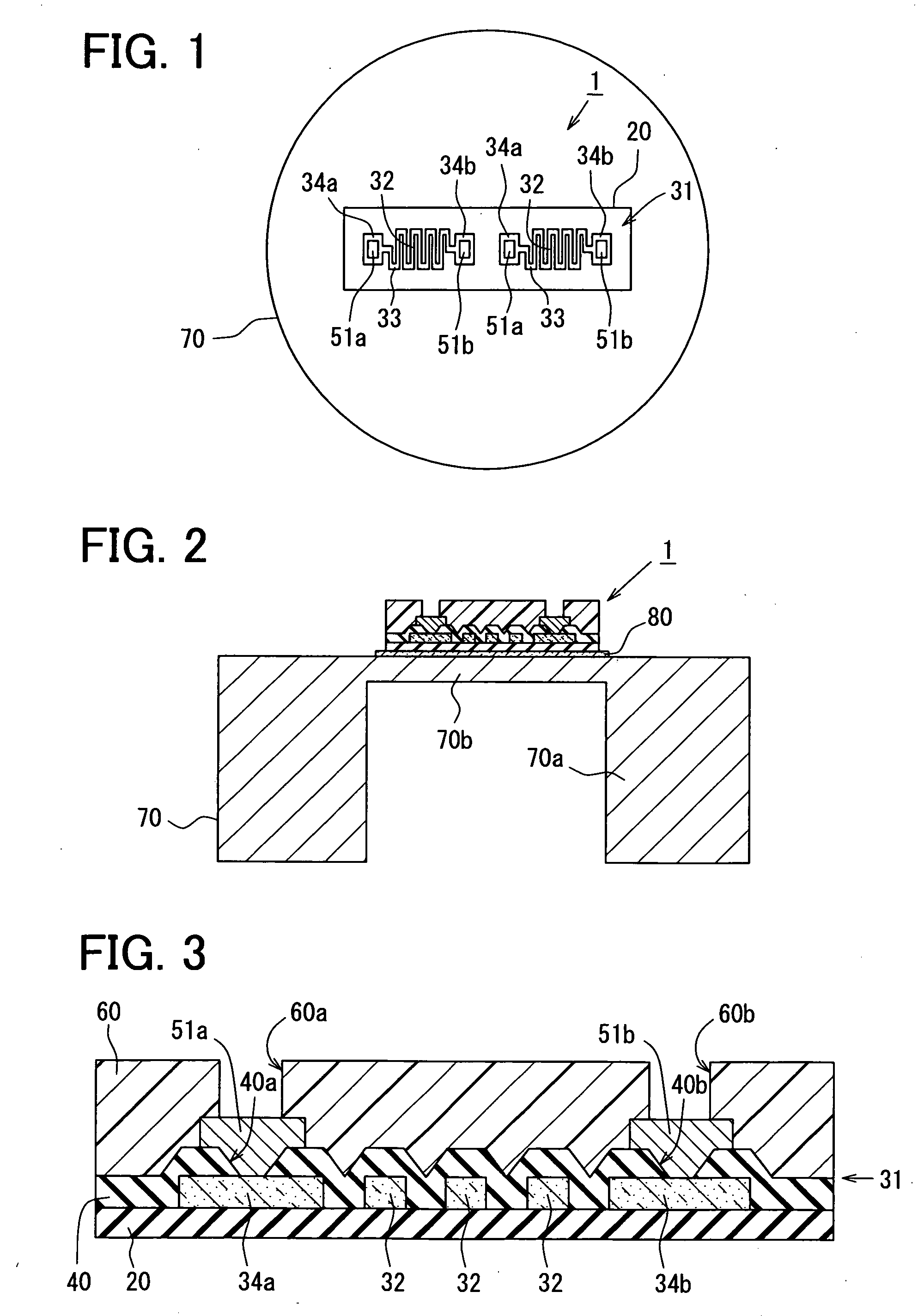
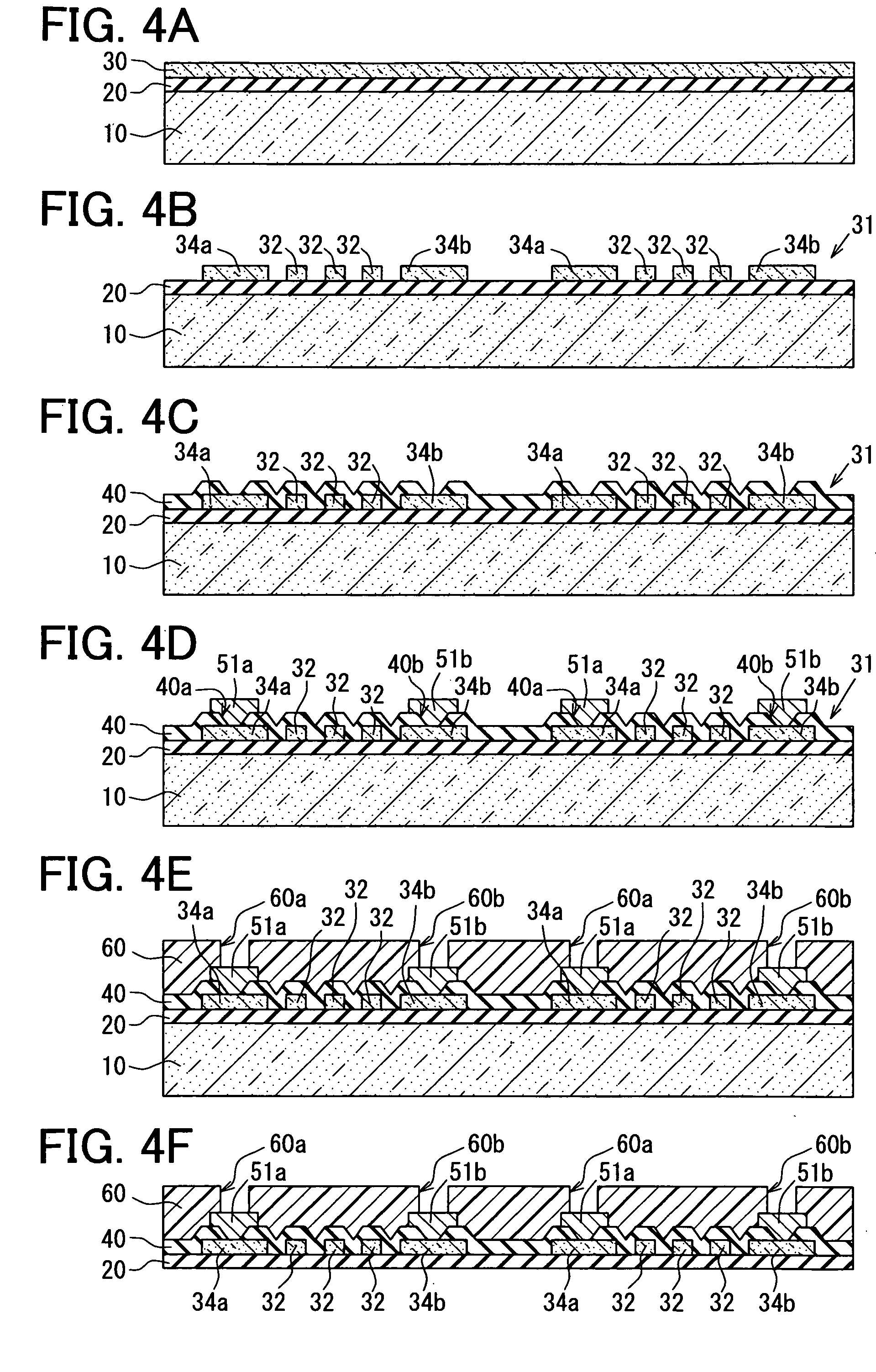
[0056]Since the stem 70 is made of a metallic material, the insulating layer 20 is left to provide an electrical insulation between the gauge section 31 and the stem 70. Alternatively, when the electrical insulation between the gauge section 31 and the stem 70 is ensured without the insulating layer 20, the insulating layer 20 can be removed as illustrated in FIG. 5, which corresponds to FIG. 4F. For example, the insulating layer 20 can be gradually removed by mechanical...

second embodiment

[0068]A pressure sensing apparatus 200 according to a second embodiment of the present invention is described below with reference to FIGS. 10, 11. For example, the pressure sensing apparatus 200 is installed to a fuel pipe (not shown) of a fuel injection system (e.g., common-rail system) of a vehicle and used to detect pressure of fuel in the fuel pipe.

[0069]As shown in FIG. 10, the pressure sensing apparatus 200 includes a housing 110 having an outer surface provided with a screw thread 111. The housing 110 is directly fixed to the fuel pipe by means of the screw thread 111. A pressure passageway 112 is formed inside the housing 110. The pressure passageway 112 has a first side (i.e., bottom side of FIG. 10) provided with a pressure inlet port for introducing the pressure into the pressure passageway 112 and a second side (i.e., top side of FIG. 10) provided with a stem room 114. When the housing 110 is fixed to the fuel pipe, the pressure passageway 112 communicates with an insid...

third embodiment

[0093]A third embodiment of the present invention is described below with reference to FIG. 14. A difference between the second and third embodiment is as follows. According to the third embodiment, a thickness L1 of the diaphragm 121 is set equal to a thickness L2 of the sensor chip 130. Specifically, after the strain gauge 132 and the insulation film 133 are formed to the front surface of the silicon substrate 131, the back surface of the silicon substrate 131 is grinded or polished until the thickness L1 of the diaphragm 121 becomes equal to the thickness L2 of the sensor chip 130.

[0094]The sensor chip 130 and the diaphragm 121 are thermally expanded and shrunk, when the pressure sensing apparatus 200 is manufactured and receives pressure. As a result, while one of the sensor chip 130 and the diaphragm 121 receives extensive stress, the other of the sensor chip 130 and the diaphragm 121 receives compressive stress. The sensor chip 130 and the diaphragm121 have a similar Young's m...


PUM

PropertyMeasurementUnit
Thicknessaaaaaaaaaa
Thicknessaaaaaaaaaa
Thicknessaaaaaaaaaa

Abstract

A semiconductor pressure sensing apparatus includes a metallic stem having a diaphragm and a semiconductor sensor bonded to the diaphragm. The semiconductor sensor includes a gauge section and first and second bonding pads. The gauge section is configured to be deformed according to a deformation of the diaphragm. The first and second bonding pads are respectively connected to different positions of the gauge section so that an electrical resistance between the first and second bonding pads can change with a change in the deformation of the diaphragm. The gauge section is formed to a semiconductor layer of an silicon-on-insulator substrate. The semiconductor sensor is directly bonded to the diaphragm by activating contact surfaces between the semiconductor sensor and the diaphragm.

Description

CROSS REFERENCE TO RELATED APPLICATION[0001]This application is based on and incorporates herein by reference Japanese Patent Applications No. 2007-19316 filed on Jan. 30, 2007 and No. 2007-31413 filed on Feb. 12, 2007.FIELD OF THE INVENTION[0002]The present invention relates to a semiconductor sensor and a method of manufacturing the semiconductor sensor.BACKGROUND OF THE INVENTION[0003]In a semiconductor pressure sensor disclosed in U.S. Pat. No. 6,635,910, a heavily-doped region serving as a gauge section is formed to a surface portion of a semiconductor substrate by an ion-implantation process, a thermal diffusion process, and the like. The semiconductor substrate of the semiconductor pressure sensor is attached to a thinned portion of an object to be detected. When receiving pressure, the thinned portion of the object is deformed according to an amount of the received pressure. The semiconductor substrate (i.e., the gauge section) attached to the thinned portion is deformed acc...

Claims


Application Information

Patent Timeline
IPC IPC(8): G01L9/04H01C17/28
CPCG01K5/52Y10T29/49103G01L9/0055G01L1/2293H01L2224/02166
Inventor YOKURA, HISANORIISOBE, YOSHIHIKOKAWASAKI, EISHI
Owner DENSO CORP
Why Eureka
Try Eureka