Semiconductor device and production method therefor

a technology of semiconductors and production methods, applied in the direction of semiconductor devices, basic electric elements, electrical appliances, etc., can solve the problems of difficult to ignore, the operation current does not rise satisfactorily, and the gate leakage current is considerable, and achieves the effect of low power consumption and fast operation

Inactive Publication Date: 2008-08-28
GK BRIDGE 1
View PDF15 Cites 7 Cited by
  • Summary
  • Abstract
  • Description
  • Claims
  • Application Information

AI Technical Summary

Benefits of technology

[0007]An object of the present invention is to provide a semiconductor device comprising a MISFET which is capable of fast operation with low power consumption while having a minute structure with a short gate length and a production method therefor.
[0078]In the present invention, there is provided a semiconductor device which comprises a MISFET capable of fast operation with low power consumption while having a minute structure with a short gate length.

Problems solved by technology

Following this, however, the amount of the gate leakage current has become considerable, which is difficult to ignore from the viewpoint of the power consumption.
However, even with the structure designed in due consideration for the reactivities of the High-K materials as in the afore-mentioned conventional technique, when the gate length becomes shortened further along with the miniaturization of the device, there arises a problem that the operation current does not rise satisfactorily in comparison with the MOSFET wherein a silicon oxide film is used as the gate insulating film.
Because the fact that the lower the Si content ratio is, the more the ON-current falls down trade off another fact that the lower the Si content ratio is, the higher the dielectric constant becomes, substantial difficulties are brought about in respect of achieving fast operations.

Method used


Image

  • Semiconductor device and production method therefor
  • Semiconductor device and production method therefor
  • Semiconductor device and production method therefor

Examples


first embodiment

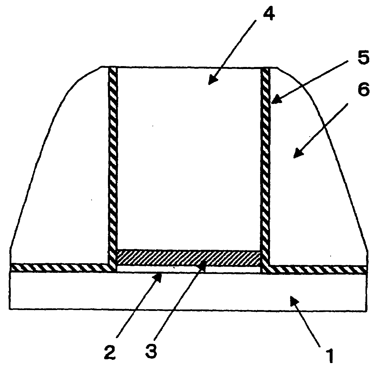
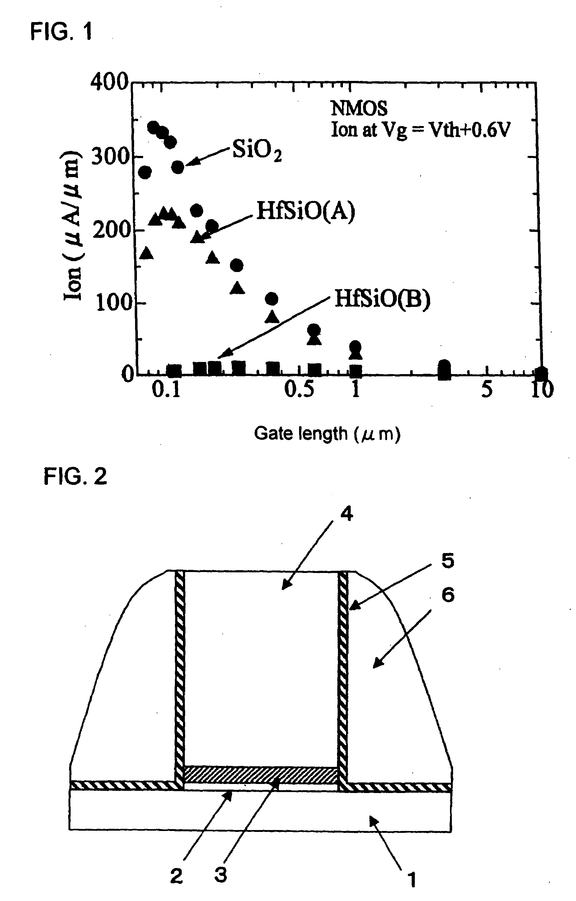
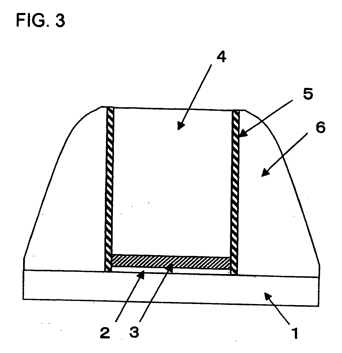
[0099]In the present embodiment, as shown in FIG. 2, there are set, on a silicon substrate 1, a gate insulating film in which layers of a silicon containing insulating film 2 and a high-dielectric-constant metal oxide film 3 are laid in this order, a silicon containing gate electrode 4 formed on this gate insulating film, and sidewalls 6 each of which is formed on a lateral face of this gate electrode, the face of which is perpendicular to the substrate and includes a lateral face of this gate insulating film, with a silicon nitride film 5 lying therebetween. In this embodiment, each of the lateral faces (the faces perpendicular to the substrate) of the high-dielectric-constant metal oxide film 3 is covered with the silicon nitride film 5.

[0100]While the silicon nitride film 5 is laid beneath each sidewall 6 in the structure shown in FIG. 2, it is also possible to have the structure in which no silicon nitride film is present beneath the sidewall (between the sidewall and the silico...

second embodiment

[0119]In the present embodiment, as shown in FIG. 5, there are set, on a silicon substrate 1, a gate insulating film in which layers of a silicon containing insulating film 2 and a high-dielectric-constant metal oxide film 3 are laid in this order, a silicon containing gate electrode 4 formed on this gate insulating film, and sidewalls 6 each of which is formed of silicon oxide on a lateral face of this gate electrode, the face of which is perpendicular to the substrate, with a silicon oxide film 7 and a silicon nitride film 5 lying in this order therebetween. Excepting that the silicon oxide films 7 are set, the structure of the present embodiment can be the same as that of First Embodiment.

[0120]While the silicon nitride film 5 is laid beneath each sidewall 6 in the structure shown in FIG. 5, it is also possible to have a structure in which no silicon nitride film is present beneath the sidewall (between the sidewall and the silicon substrate) as shown in FIG. 6. Compared with the...

third embodiment

[0127]In the present embodiment, as shown in FIG. 8, there are set, on a silicon substrate 1, a gate insulating film in which layers of a silicon containing insulating film 2 and a high-dielectric-constant metal oxide film 3 are laid in this order, a silicon containing gate electrode 4 formed on this gate insulating film, silicon nitride films 51 (nitrogen-containing sections) each of which is formed selectively and directly on a lateral face of this gate insulating film and sidewalls 6 each of which is formed of silicon oxide on a lateral face of this gate electrode, the face of which is perpendicular to the substrate and includes the surface of this silicon nitride film 51. Each silicon nitride film 51 covers the internal faces of a recess that is formed with respect to the plane of a lateral face of the gate electrode, so as to fill up the recess. The thickness of these silicon nitride films 51 may be set appropriately within a range enough to provide the barrier function against...


PUM


Abstract

A semiconductor device provided with a MIS type field effect transistor comprising a silicon substrate, a gate insulating film having a high-dielectric-constant metal oxide film which is formed on the silicon substrate via a silicon containing insulating film, a silicon-containing gate electrode formed on the gate insulating film, and a sidewall including, as a constituting material, silicon oxide on a lateral face side of the gate electrode, wherein a silicon nitride film is interposed between the sidewall and at least the lateral face of the gate electrode. This semiconductor device, although having a fine structure with a small gate length, is capable of low power consumption and fast operation.

Description

CROSS REFERENCE TO RELATED APPLICATIONS[0001]The present Application is a Divisional Application of U.S. patent application Ser. No. 10 / 561,608 filed on Dec. 20, 2005.TECHNICAL FIELD[0002]The present invention relates to a semiconductor device and a production method therefor, and more particularly to a semiconductor device having a MIS type field effect transistor (MISFET) wherein a film of a highly dielectric substance is used as a gate insulating film and a production method therefor.BACKGROUND ART[0003]In recent years, for the purpose of providing the MOS type field effect transistor (MOSFET) with a higher operation speed, attempts to make the gate insulating film (SiO2 film) thinner has been being made, achieving a thickness of 2 nm or so. Following this, however, the amount of the gate leakage current has become considerable, which is difficult to ignore from the viewpoint of the power consumption. In order to reduce the amount of this gate leakage current, the use of a materi...

Claims


Application Information

Patent Timeline
Patent Type & Authority Applications(United States)
IPC IPC(8): H01L29/78H01L21/28H01L29/51
CPCH01L21/28185H01L21/28194H01L21/28211H01L29/78H01L29/517H01L29/518H01L29/6656H01L29/513
Inventor OGURA, TAKASHIIKARASHI, NOBUYUKIIWAMOTO, TOSHIYUKIWATANABE, HIROHITO
Owner GK BRIDGE 1
Why Eureka
Try Eureka