Flat panel display apparatus with grounded PCB

a technology of display apparatus and control pcb, which is applied in the direction of non-linear optics, identification means, instruments, etc., can solve the problems of deteriorating picture being displayed, affecting the performance of lcd, and difficult to ground the control pcb in the above-described manner

Active Publication Date: 2008-08-28
SAMSUNG DISPLAY CO LTD
View PDF10 Cites 12 Cited by
  • Summary
  • Abstract
  • Description
  • Claims
  • Application Information

AI Technical Summary

Benefits of technology

[0014]Accordingly, it is an aspect of the present invention to provide a flat panel display apparatus in which a control PCB having the length shorter than the width of a flat panel display module is easily grounded.

Problems solved by technology

While the LCD operates, the control PCB produces an EMI (electromagnetic interference) disturbing the performance of the LCD, e.g., deteriorating the picture being displayed.
However, if the LCD has the control PCB whose length is shorter than the width of the flat panel display module, it is difficult to ground the control PCB in the above-described manner.
For example, in the case of the COG type LCD, the control PCB is placed in the middle of the rear edge area of the flat panel display module, and the FPC has the width shorter than that of the flat panel display module and is placed in the middle of the edge of the flat panel, so that it is difficult to ground the control PCB in the above-described manner using the screws.

Method used


Image

  • Flat panel display apparatus with grounded PCB
  • Flat panel display apparatus with grounded PCB
  • Flat panel display apparatus with grounded PCB

Examples


Embodiment Construction

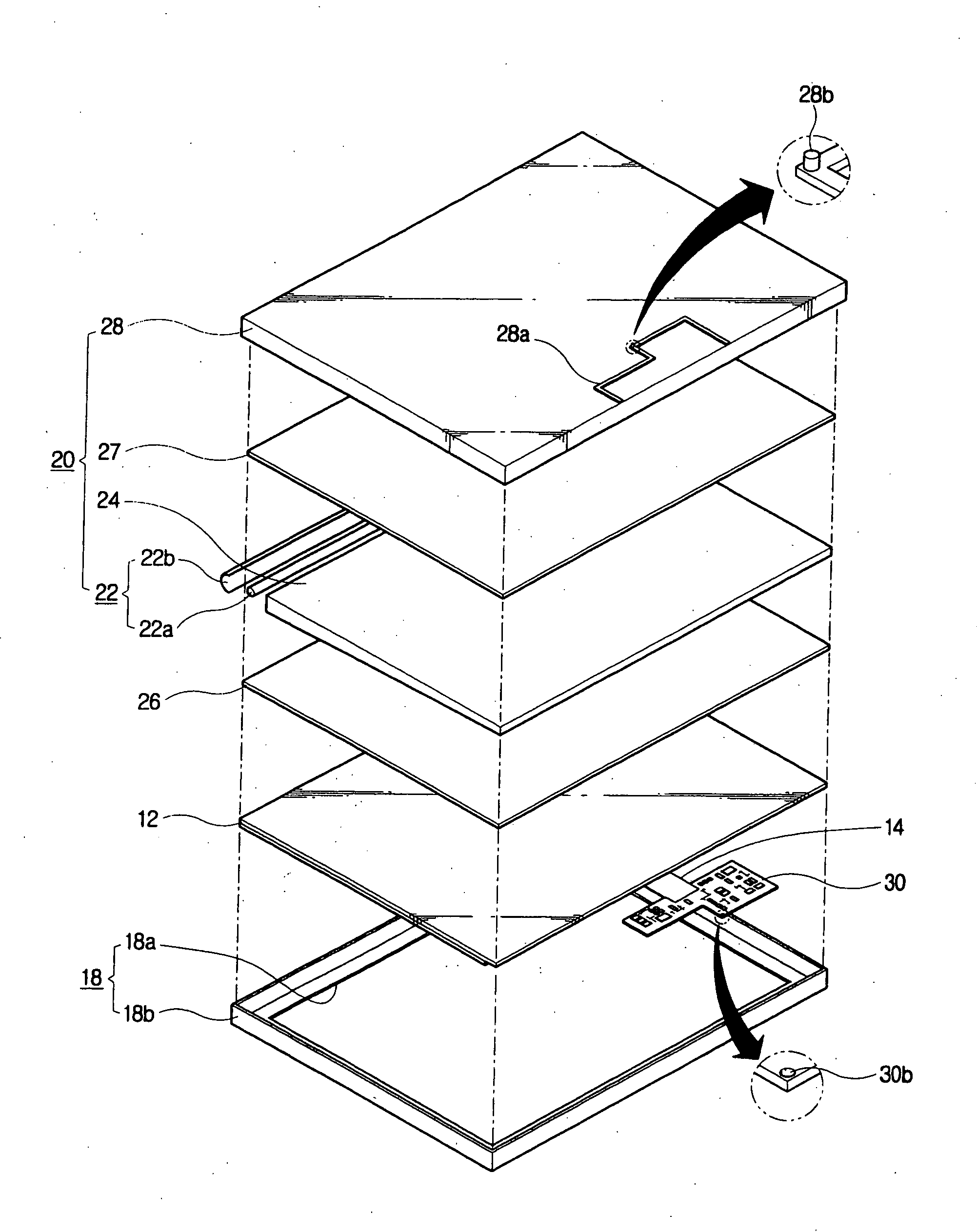
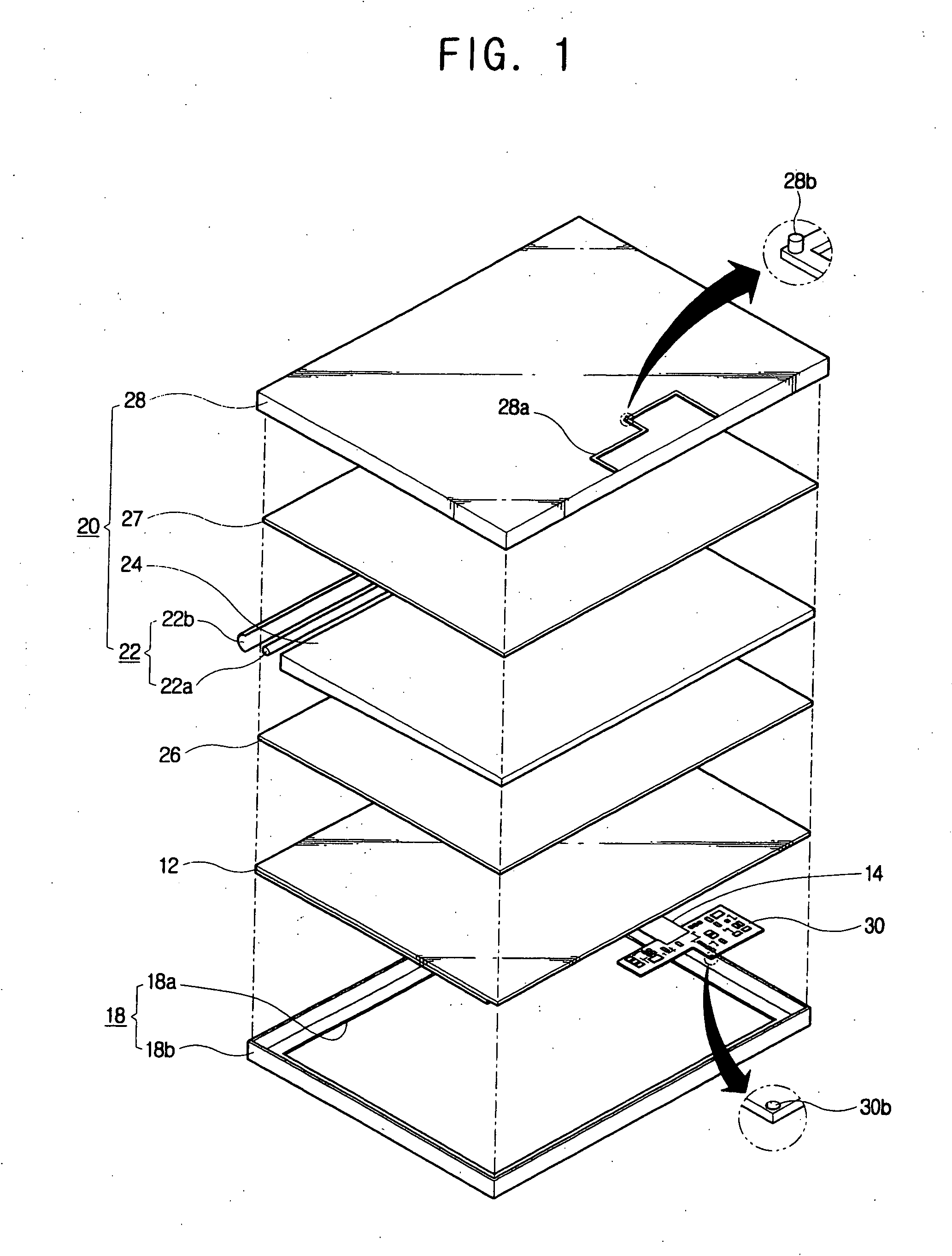
[0032]Reference will now made in detail to the embodiments of the present invention, examples of which are illustrated in the accompanying drawings, wherein like reference numerals refer to like elements throughout. The embodiments are described below in order to explain the present invention by referring to the figures.

[0033]In these embodiments, a COG type LCD will be exemplarily described as a flat panel display apparatus.

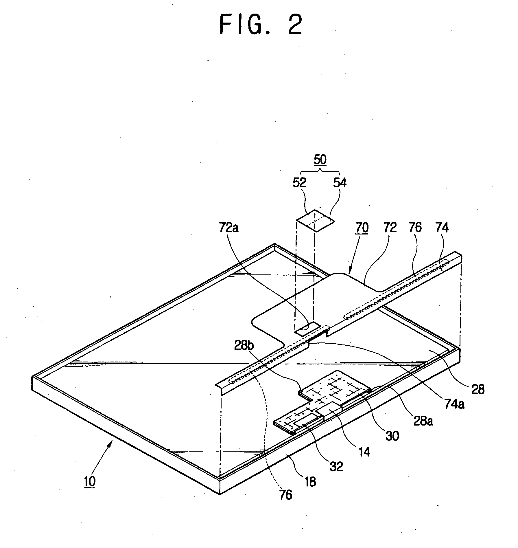
[0034]As shown in FIGS. 1 and 2, a COG type LCD according to the present invention comprises a flat panel display module 10 on which a picture is displayed; a control PCB 30 placed in one rear edge area of the flat panel display module 10 and provided with a conductive grounding part 32 on the rear surface thereof; and a grounding contact member 50 allowing the grounding part 32 of the control PCB 30 to contact the flat panel display module 10. The flat panel display module 10 and the control PCB 30 are covered with front and rear cases (not shown), to thereby b...


PUM

PropertyMeasurementUnit
areaaaaaaaaaaa
adhesiveaaaaaaaaaa
conductiveaaaaaaaaaa

Abstract

A flat panel display apparatus comprises a flat panel display module; a control PCB placed in one rear edge area of the flat panel display module and having a conductive grounding part; and a grounding contact member including a rear contact part contacting the grounding part of the control PCB, and a side contact part bent from the rear contact part and contacting one edge of the flat panel display module, and grounding the control PCB. With this configuration, the present invention provides a flat panel display apparatus in which a control PCB having the length shorter than the width of a flat panel display module is easily grounded and the production cost thereof is decreased.

Description

CROSS-REFERENCE TO RELATED APPLICATIONS[0001]This application is a continuation of U.S. patent application Ser. No. 10 / 747,672, filed Dec. 30, 2003, by Sang-Duk Lee, entitled “FLAT PANEL DISPLAY APPARATUS,” which claims priority of Korean Patent Application No. 2002-0086901, filed Dec. 30, 2002, in the Korean Intellectual Property Office, the disclosures of which are incorporated herein by reference.BACKGROUND OF THE INVENTION[0002]1. Field of the Invention[0003]The present invention relates to a flat panel display apparatus, and more particularly, to a flat panel display apparatus improved in a grounding structure of a control PCB (printed circuit board).[0004]2. Description of the Related Art[0005]A flat panel display apparatus includes an LCD (liquid crystal display), a PDP (plasma display panel), a VFD (vacuum fluorescent display), an FED (field emission display), an ELD (electro luminescence display), etc.[0006]Making of the LCD includes arranging a plurality of TFTs (thin film...

Claims


Application Information

Patent Timeline
Patent Type & Authority Applications(United States)
IPC IPC(8): G02F1/1333G02F1/13G02F1/1345G09F9/00
CPCG02F1/13452G02F1/1345
Inventor LEE, SANG-DUK
Owner SAMSUNG DISPLAY CO LTD
Why Eureka
Try Eureka