Supercharge Your Innovation With Domain-Expert AI Agents!

Memory Controller, Control Method For Accessing Semiconductor Memory And System

a memory controller and control method technology, applied in the field of memory controllers controlling access to semiconductor memory, can solve the problems of insufficient improvement of access efficiency and inability to improve access efficiency, and achieve the effect of improving access efficiency

Active Publication Date: 2008-08-28
SOCIONEXT INC
View PDF5 Cites 2 Cited by
  • Summary
  • Abstract
  • Description
  • Claims
  • Application Information

AI Technical Summary

Benefits of technology

[0010]According to one aspect of the embodiment, a memory controller accessing a semiconductor memory sequentially holds access requests which include access addresses each indicating a memory cell to be accessed and which are supplied from a system controller. The semiconductor memory includes a plurality of banks each having a plurality of pages. The memory controller decides page hit / page miss of the bank corresponding to each of the plural held access addresses. Further, the memory controller outputs an all-banks precharge command for performing a precharge operation of all the banks when deciding, based on an analysis of the plural access addresses, that outputting the all-banks precharge command results in improvement in access efficiency.

Problems solved by technology

Therefore, in the entire memory including a plurality of banks, access efficiency is not improved.
As a result, access efficiency cannot be sometimes improved sufficiently.

Method used


Image

  • Memory Controller, Control Method For Accessing Semiconductor Memory And System
  • Memory Controller, Control Method For Accessing Semiconductor Memory And System
  • Memory Controller, Control Method For Accessing Semiconductor Memory And System

Examples


first embodiment

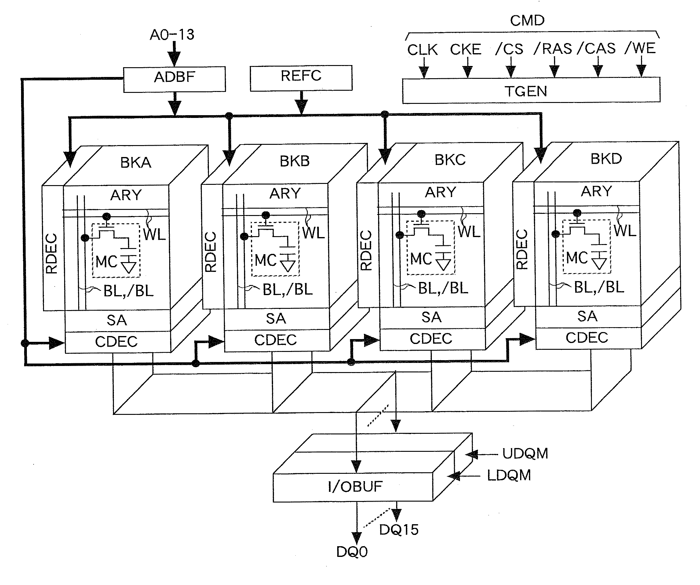
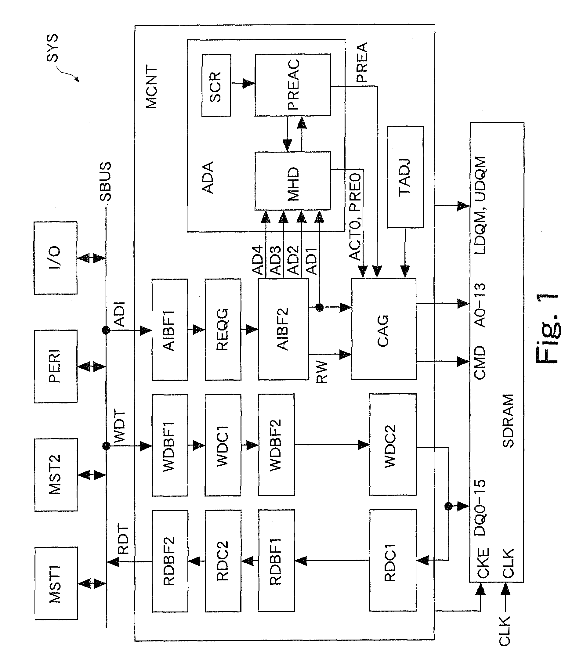
[0029]FIG. 1 shows a In this embodiment, a system SYS has: master controllers MST1, MST2 (system controllers), a peripheral circuit PERI, an input / output interface I / O, and a memory controller MCNT which are connected to a system bus SBUS; and a SDRAM (semiconductor memory) accessed by the memory controller MCNT. The master controllers MST1, MST2 are CPUs, DMACs, or the like controlling the operation of the whole system SYS. The peripheral circuit PERI is, for example, an image control circuit such as a MPEG controller. The input / output interface I / O is, for example, a USB interface circuit. The SDRAM has four banks BKA, BKB, BKC, BKD each having a plurality of pages. FIG. 5 shows details of the SDRAM.

[0030]The system SYS is configured by, for example, a control board of a mobile phone, a digital camera, or the like. For example, the master controllers MST1, MST2, the peripheral circuit PERI, the input / output interface I / O, and the memory controller MCNT are formed on one LSI chip ...

third embodiment

[0083]FIG. 17 shows the operations of the memory controller MCNT and the SDRAM in the In this example, by the process flow shown in FIG. 16, the activate command ACT in response to each of the second to fourth access requests is insertable between the activate command ACT and the read command RD.

[0084]The foregoing third embodiment can also provide the same effects as those of the above-described first embodiment. In addition, in this embodiment, the activate command ACT in response to each of the second to fourth access requests is inserted between the activate command ACT and the read command RD by the address analysis unit ADA, which enables further improvement in access efficiency.

[0085]The above embodiments have described the examples applied to the SDRAM operating in synchronization with clocks. For example, the present embodiments may be applied to a clock-asynchronous DRAM. The SDRAM and the DRAM may be in a chip form or may be macros mounted on a SoC.

[0086]The above embodi...


PUM


Abstract

A memory controller sequentially holds access requests including access addresses. A semiconductor memory includes a plurality of banks each having a plurality of pages. The memory controller decides page hit / page miss of the bank corresponding to each of the held access addresses. Further, the memory controller outputs an all-banks precharge command for performing a precharge operation of all the banks when deciding, based on an analysis of the successive access addresses, that outputting the all-banks precharge command results in improvement in access efficiency. It is possible to precharge the plural banks only by supplying the all-banks precharge command once, and therefore, in a case where the number of empty cycles for the insertion of a command is small, it is possible to supply the command efficiently to the semiconductor memory according to the states of the banks.

Description

CROSS-REFERENCE TO RELATED APPLICATION[0001]This application is based upon and claims the benefit of priority from Japanese Patent Application No. 2007-045233, filed on Feb. 26, 2007, the entire contents of which are incorporated herein by reference.BACKGROUND[0002]1. Field[0003]The present embodiments relate to a memory controller controlling access to a semiconductor memory, and relates to a system.[0004]2. Description of the Related Art[0005]For improving access efficiency, many of semiconductor memories such as SDRAMs have a plurality of banks capable of independent operation. In order to access a memory cell in a semiconductor memory of this type, it is necessary to supply an activate command, a read or write command, and a precharge command. The activate command is a command for selecting a word line and latching, in a sense amplifier, data held in memory cells connected to the selected word line. The read command is a command for reading the data latched in the sense amplifie...

Claims


Application Information

Patent Timeline
Patent Type & Authority Applications(United States)
IPC IPC(8): G06F12/00
CPCG06F12/0215G11C11/408G11C11/4093G11C11/4074
Inventor HARA, SOJI
Owner SOCIONEXT INC
Features
  • R&D
  • Intellectual Property
  • Life Sciences
  • Materials
  • Tech Scout
  • Unparalleled Data Quality
  • Higher Quality Content
  • 60% Fewer Hallucinations
Learn More