Drive method of plasma display panel
a technology of plasma display panel and drive method, which is applied in the direction of instruments, static indicating devices, and address electrodes, etc., can solve the problems of increasing the possibility of discharge failure and the inability to significantly increase the dark contrast, and achieve the effect of increasing the dark contras
- Summary
- Abstract
- Description
- Claims
- Application Information
AI Technical Summary
Benefits of technology
Problems solved by technology
Method used
Image
Examples
embodiment 1
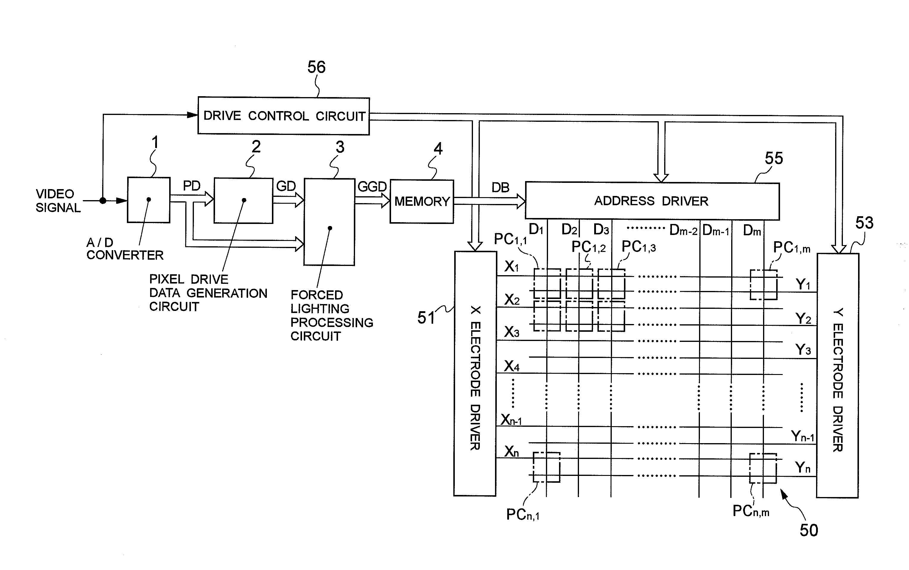
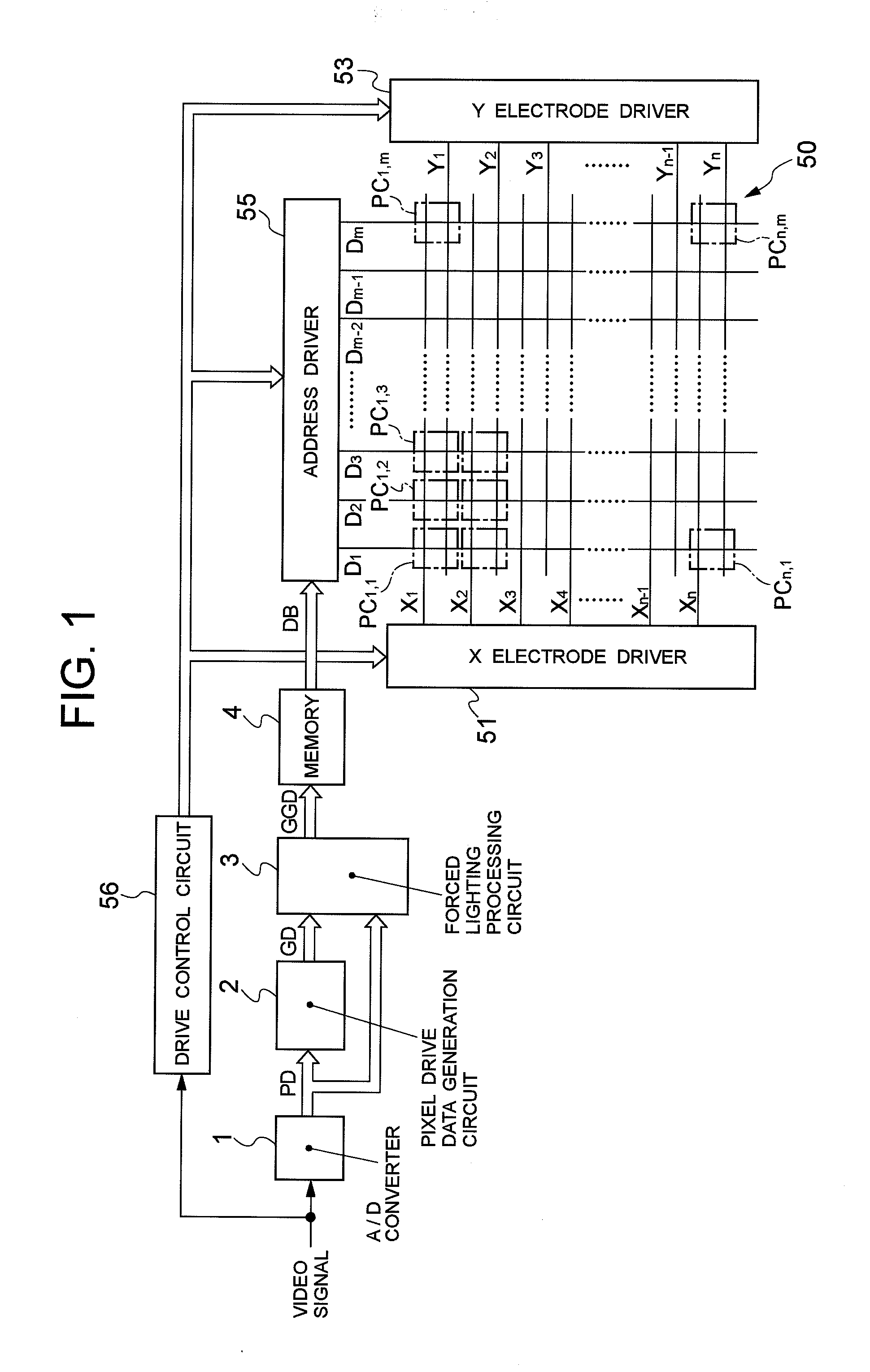
[0044]FIG. 1 shows a schematic configuration of the plasma display device in accordance with the present invention.
[0045]As shown in FIG. 1, the plasma display device is composed of an A / D converter 1, a pixel drive data generation circuit 2, a forced lighting processing circuit 3, a memory 4, a PDP 50, an X electrode driver 51, an Y electrode driver 53, an address driver 55, and a drive control circuit 56.
[0046]The A / D converter 1 samples the input video signal, converts it into, for example, 8-bit pixel data PD corresponding to each pixel, and supplies the data to the pixel drive data generation circuit 2 and forced lighting processing circuit 3.
[0047]The pixel drive data generation circuit 2, first, performs a multigradation processing including an error diffusion processing and a dither processing with respect to each pixel data PD of each pixel. For example, in the error diffusion processing, the pixel drive data generation circuit 2 takes higher-level 6-bit portion of pixel da...
embodiment 2
[0179]FIG. 25 shows the configuration of a plasma display device created with consideration for the above-described issues.
[0180]The configuration of the plasma display device shown in FIG. 25 is identical to that shown in FIG. 1, except that a pixel drive data generation circuit 20 is provided instead of the pixel drive data generation circuit 2 shown in FIG. 1, a forced lighting processing circuit 30 is provided instead of the forced lighting processing circuit 3, and a drive control circuit 560 is provided instead of the drive control circuit 56.
[0181]Therefore, the explanation below will be focused on the operation of the pixel drive data generation circuit 20, forced lighting processing circuit 30, and drive control circuit 560.
[0182]First, the pixel drive data generation circuit 20 performs a multigradation processing including an error diffusion processing and a dither processing with respect to 8-bit pixel data PD supplied from the A / D converter 1, in the same manner as in t...
PUM
 Abstract
Description
Claims
Application Information


