Image pixel employing floating base readout concept, and image sensor and image sensor array including the image pixel

Active Publication Date: 2008-09-04
INTELLECTUAL VENTURES II
View PDF18 Cites 23 Cited by
  • Summary
  • Abstract
  • Description
  • Claims
  • Application Information

AI Technical Summary

Benefits of technology

[0009]Another specific embodiment of the present invention is directed toward providing a CMOS image sensor using pinned photodiodes for light sensing in conjunction with floating base bipolar transistors incorporated in each pixel, so as to obtain a charge gain, which results in an increase of pixel sensitivity and simultaneously decrease in noise.
[0010]Still another specific embodimen

Problems solved by technology

This step removes the collected charge; however, it generates kTC-reset noise as is well known in the art.
Although it is possible to share some of these lines and corresponding transistors between neighboring pixels, this sharing may generate other com

Method used


Image

  • Image pixel employing floating base readout concept, and image sensor and image sensor array including the image pixel
  • Image pixel employing floating base readout concept, and image sensor and image sensor array including the image pixel
  • Image pixel employing floating base readout concept, and image sensor and image sensor array including the image pixel

Examples


Embodiment Construction

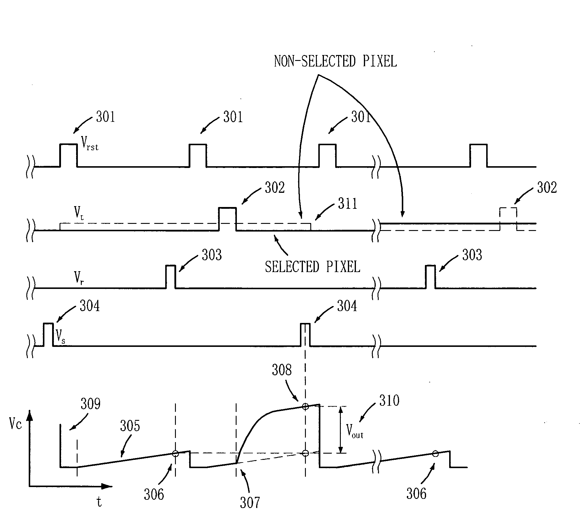
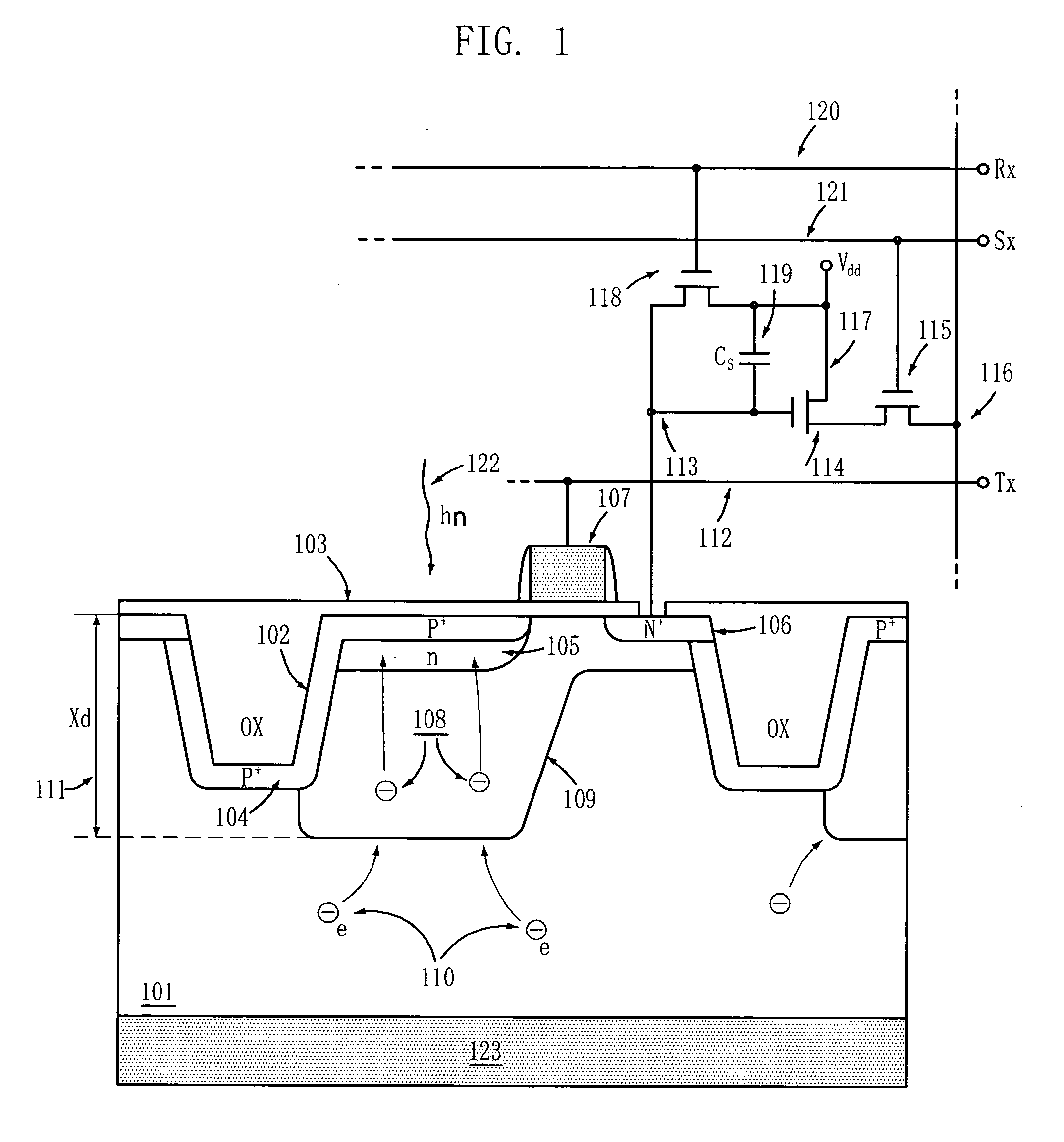
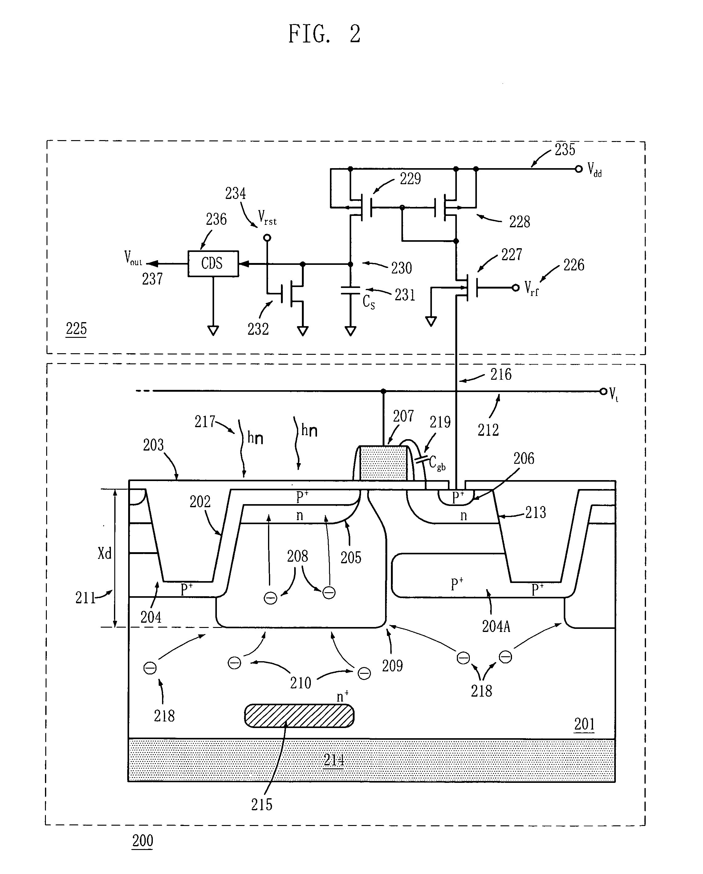
[0018]Various embodiments of the present invention provide a different approach to building small pixel size CMOS image sensors that can address the difficulties associated with the conventional approach. In particular, specific embodiments of the present invention provide small pixels with improved charge storage capacity, increased optical aperture response, and increased sensitivity.

[0019]By eliminating reset and address transistors from the pixels and by replacing a charge sensing transistor with a bipolar transistor that has a floating base, it is possible to operate the pixels with one row address line and one column output line. The column output line is common to all pixel emitters in one column, so that no addressing transistor is required. Furthermore, by incorporating the bipolar transistor into the pixel, a significant charge gain can be obtained before a signal is transferred onto the column output line, and thus, the sensor sensitivity can be substantially increased. S...


PUM


Abstract

A pixel of an image sensor includes only two signal lines per pixel, a pinned photodiode for sensing light, a floating base bipolar transistor, and no reset and address transistors. The floating base bipolar transistor provides the pixel with a gain, which can increase pixel sensitivity and reduce noise. The pixel also incorporates a vertical blooming control structure for an efficient blooming suppression. The output terminals of the pixel are coupled to a common column output line terminated by a special current sensing correlated double sampling circuit, which is used for subtraction of emitter leakage current. Based on this structure, the pixel has high sensitivity, high response uniformity, low noise, reduced size, and efficient layout.

Description

CROSS-REFERENCE TO RELATED APPLICATIONS[0001]The present invention claims priority of Korean patent application number 10-2006-0132634, filed on Dec. 22, 2006, which is incorporated by reference in its entirety.BACKGROUND OF THE INVENTION[0002]The present invention relates to an image sensor, and more particularly, to an image sensor with high resolution, high performance and small pixel sizes. For this purpose, the present invention provides a pixel having a vertical blooming, one address line and one column output line per pixel without having additional charge transfer and reset lines. The present invention also provides a pixel having an integrated bipolar transistor gain stage where charge received from a pinned diode is multiplied several times before a signal is transferred on a common column output line and processed by a current sensing column correlated double sampling (CDS) circuit.[0003]Typical image sensors sense light by converting impinging photons into electrons that...

Claims


Application Information

Patent Timeline
IPC IPC(8): H04N5/335H01L27/148H01L27/146H04N5/357H04N5/369H04N5/374
CPCH01L27/14603H01L27/14609H01L27/1463H01L27/14656H01L31/035281H04N3/1568H03K17/20H04N5/3591H04N5/363H04N5/3741H04N5/3745H01L27/14605H04N5/3575H04N25/621H04N25/616H04N25/65H04N25/766H04N25/77H01L27/146
Inventor HYNECEK, JAROSLAV
Owner INTELLECTUAL VENTURES II
Why Eureka
Try Eureka