

Method for profiling the perimeter border of a semiconductor wafer
a technology of semiconductor wafers and perimeter borders, which is applied in the direction of manufacturing tools, laser beam welding apparatus, welding/soldering/cutting articles, etc., can solve the problems of unwanted mechanical contact of each very precisely processed plane, and achieve free definable shape, better area utilization, and rapid edge processing
- Summary
- Abstract
- Description
- Claims
- Application Information
AI Technical Summary
Benefits of technology
Problems solved by technology
Method used
Image

Examples
Embodiment Construction
[0030]While this invention may be embodied in many different forms, there are described in detail herein a specific preferred embodiment of the invention. This description is an exemplification of the principles of the invention and is not intended to limit the invention to the particular embodiment illustrated.
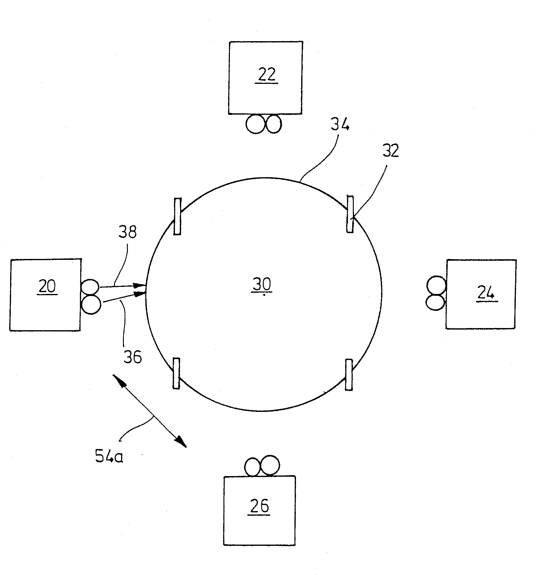
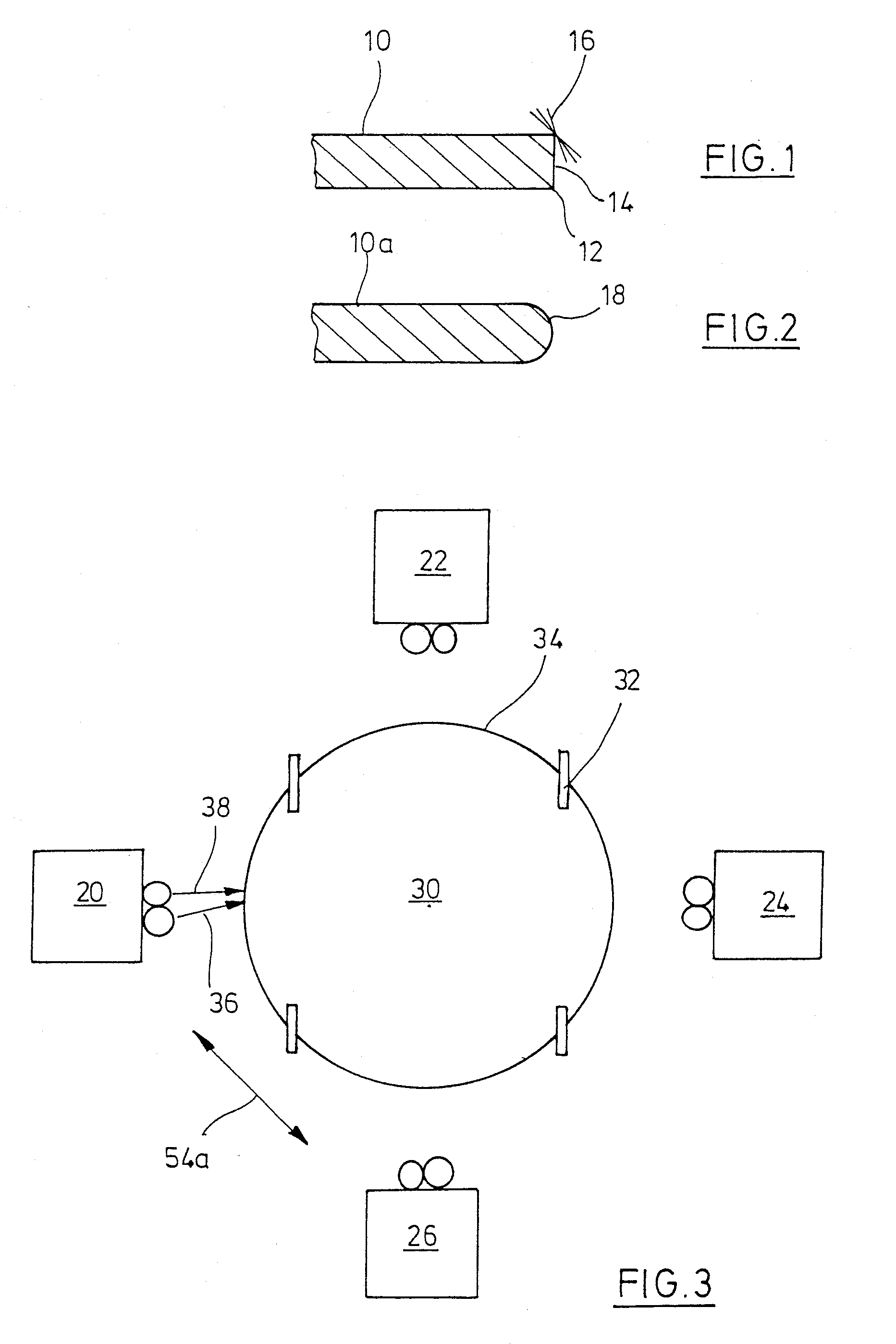
[0031]A semiconductor chip 10 in FIG. 1 is to be regarded as a flat cylinder, with relatively sharp edges 12 of its perimeter border 14. When processing of the edges 12 is performed along the lines 16, a desired profile can be imparted to the perimeter border 14. Such a profile can be recognized at 18 of the semiconductor chip 10a in FIG. 2. The apparatuses according to FIG. 3 and 5 are suited for producing such a profile.
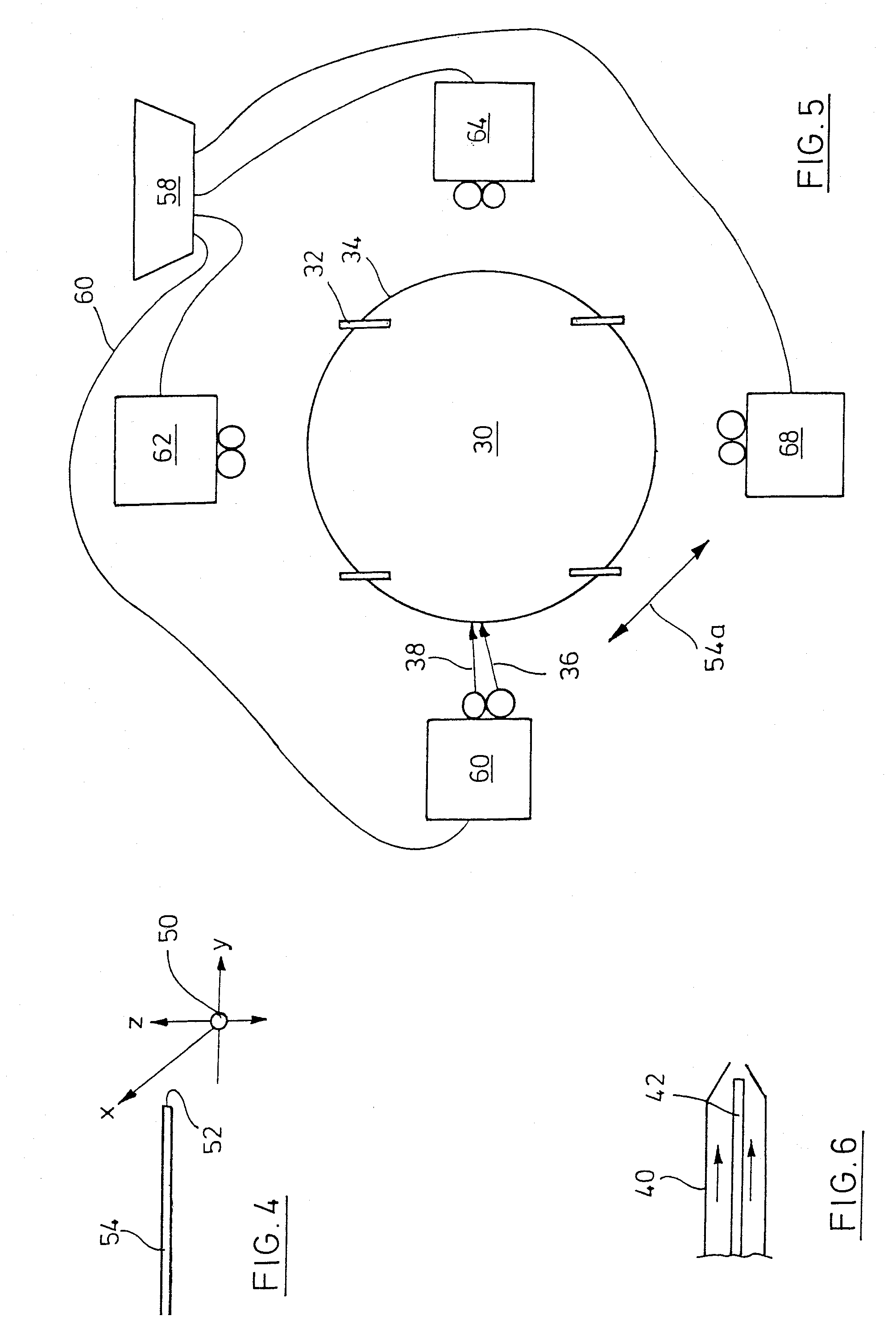
[0032]In FIG. 3, four laser units 20, 22, 24, 26 are arranged at an angle distance of 90° around a semiconductor chip 30. The semiconductor chip 30 is supported on four supporting points 32, which touch the lower surface of the semiconductor chip 30 only in ...
PUM
| Property | Measurement | Unit |
|---|---|---|
| perimeter | aaaaa | aaaaa |
| angle | aaaaa | aaaaa |
| roughness | aaaaa | aaaaa |
Abstract
Description
Claims
Application Information