Two-dimensional semiconductor detector having mechanically and electrically joined substrates

a two-dimensional semiconductor and substrate technology, applied in the direction of x/gamma/cosmic radiation measurement, instruments, radioation control devices, etc., can solve the problems of production yield and fees, bad connections, and conventional two-dimensional semiconductor detectors, so as to reduce leakage of carriers, improve detection sensitivity and spatial resolution, and reduce the effect of leakag

Inactive Publication Date: 2008-09-11
SHIMADZU CORP
View PDF6 Cites 5 Cited by
  • Summary
  • Abstract
  • Description
  • Claims
  • Application Information

AI Technical Summary

Benefits of technology

[0009]The object of the present invention is to overcome these problems and to provide a direct-conversion type two-dimensional semiconductor detector that can improve production efficiency while maintaining accuracy and a two-dimensional imaging device equipped with the same.

Problems solved by technology

However, the conventional two-dimensional semiconductor detector has the following problems.
When the detection-side substrate and the reading-side substrate are to be combined so that there are electrical connections, the split electrodes on the detection-side substrate must be precisely aligned with the reading elements on the reading-side substrate or else the split electrodes will short-circuit adjacent reading elements, resulting in bad connections.
This causes problems in terms of production yield and fees.

Method used


Image

  • Two-dimensional semiconductor detector having mechanically and electrically joined substrates
  • Two-dimensional semiconductor detector having mechanically and electrically joined substrates
  • Two-dimensional semiconductor detector having mechanically and electrically joined substrates

Examples


first embodiment

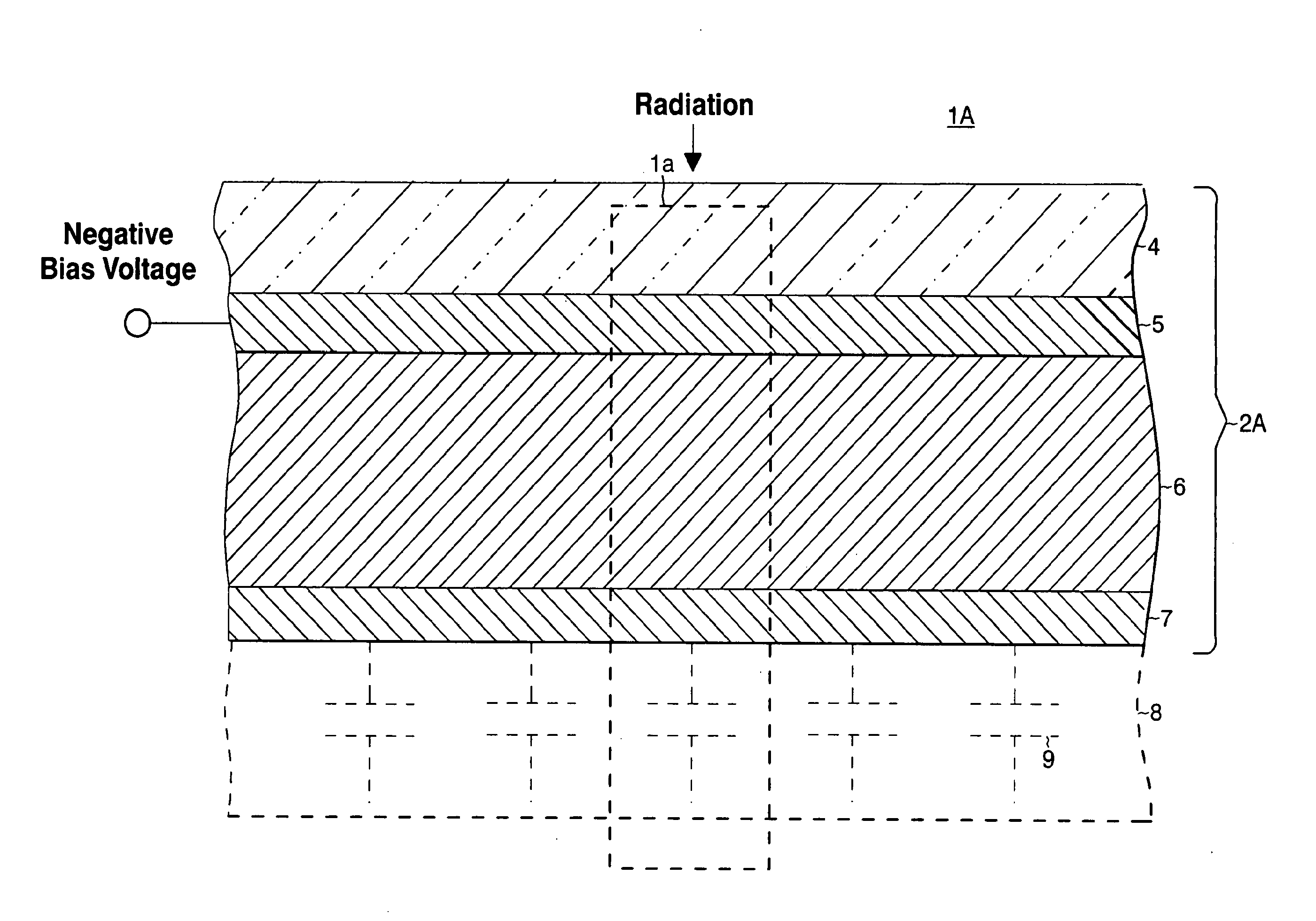
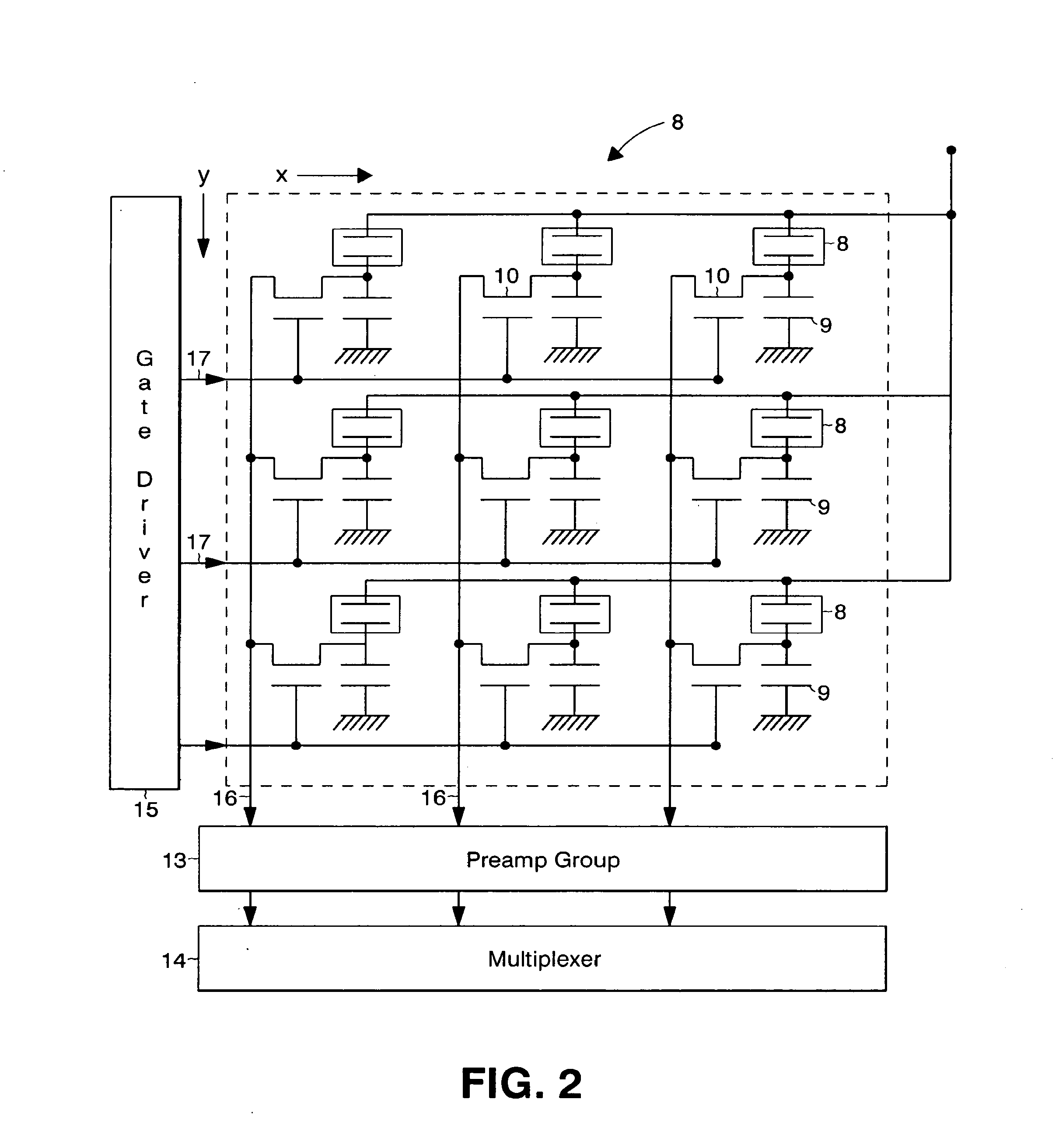
[0046]FIG. 1 is a cross-section drawing showing the structure of a two-dimensional detector according to a first embodiment. FIG. 2 is a simplified circuit diagram showing an equivalent circuit of a two-dimensional semiconductor detector according to the first embodiment. FIG. 3 is a cross-section drawing showing the structure of a single detection element according to the first embodiment.

[0047]In a two-dimensional semiconductor detector 1A according to the first embodiment, a detection module serving as a detection-side substrate (sensor substrate) for detecting light or radiation is directly stacked to a surface of a reading-side substrate (active matrix substrate) 3, which accumulates / reads generated carriers.

[0048]In a detection module 2A, carriers are generated according to a direct-conversion system in response to incoming light or radiation. The reading-side substrate 3 is set up so that the generated carriers are collected element-by-element and then retrieved. The elements...

second embodiment

[0068]Next, a two-dimensional semiconductor detector 1B according to a second embodiment will be described, with references to the figures.

[0069]FIG. 4 is a cross-section drawing showing the structure of a two-dimensional semiconductor detector according to the second embodiment. FIG. 5 is a front-view drawing showing the bonded (joined) state of the detection-side and reading-side substrates in the first embodiment. FIG. 6 is a cross-section drawing showing the structure of a single detection element according to the second embodiment.

[0070]For this embodiment, the description will cover a two-dimensional semiconductor detector in which the detection-side substrate generating carriers in response to incoming radiation and the reading-side substrate are made separately. Since only the detection substrate differs in structure from the detection module 2 from the first embodiment, like elements will be assigned like numerals and corresponding descriptions will be omitted.

[0071]As show...

third embodiment

[0078]For this embodiment, a two-dimensional imaging device equipped with the two-dimensional semiconductor detector 1A or 1B from the first and the second embodiments will be described.

[0079]FIG. 7 is a block diagram showing the overall structure of a two-dimensional imaging device according to this embodiment. The specific structure will be described based on FIG. 7. Since the structure and the like of the two-dimensional semiconductor detector 1 (1A, 1B) for detecting X-rays has already been described, detailed descriptions will be omitted here.

[0080]In the two-dimensional imaging device of this embodiment, an X-ray tube 20 that applies X rays as radiation to a body M being detected and a two-dimensional semiconductor detector 1 detecting X-rays transmitted through the body M are arranged facing each other on either side of the body M on a worktop B. In a control system at a stage coming after the two-dimensional semiconductor detector 1, a two-dimensional image of the body M is ...


PUM


Abstract

The present invention relates to an industrial or medical radiation detector and a radiation imaging device equipped with the same. More specifically, the present invention relates to a technology for improving the detection properties and production efficiency for radiation detectors. The invention in claim 1 includes: a conductive support substrate; a semiconductor sensitivity film stacked onto the support substrate and generating a carrier (electron, positive hole) in response to an item to be detected; and means for reading equipped with an element for accumulating and reading the carrier generated by the semiconductor sensitivity film.

Description

INCORPORATION BY REFERENCE[0001]The present application claims priority under 35 U.S.C. §119 to Japanese Patent Application No. 2003-179917 filed on Jun. 24, 2003. The content of the application is incorporated herein by reference in its entirety.BACKGROUND OF THE INVENTION[0002]The present invention relates to a direct conversion type two-dimensional semiconductor detector equipped with a semiconductor sensitivity film converting light or radiation directly to a carrier and a two-dimensional imaging device equipped with the same. More specifically, the present invention relates to a technology for improving production efficiency while maintaining the accuracy of the two-dimensional semiconductor detector.[0003]In recent years, two-dimensional semiconductor detectors have been used in medical and industrial fields to detect light or radiation. As shown in FIG. 9, in the case of a conventional two-dimensional semiconductor detector 51, multiple detection elements 53a are aligned vert...

Claims


Application Information

Patent Timeline
Patent Type & Authority Applications(United States)
IPC IPC(8): H01L31/18H01L31/00G01T1/00G01T1/24H01L27/00H01L27/12H01L27/14H01L27/146H01L29/786H01L31/09H01L31/115
CPCH01L27/12H01L27/14658H01L31/115H01L29/7869H01L27/14659
Inventor TOKUDA, SATOSHIKISHIHARA, HIROYUKI
Owner SHIMADZU CORP
Why Eureka
Try Eureka