Method of producing organic light emitting device

a light emitting device and organic technology, applied in the manufacture of electrode systems, cold cathode manufacturing, electric discharge tube/lamp manufacture, etc., can solve the problems of reducing affecting the sealing performance of the device, so as to achieve excellent sealing performance, reduce degradation, and improve the sealing performance

Inactive Publication Date: 2008-09-25
CANON KK
View PDF8 Cites 27 Cited by
  • Summary
  • Abstract
  • Description
  • Claims
  • Application Information

AI Technical Summary

Benefits of technology

[0016]According to the present invention, a short-circuited site is specified with respect to an organic light emitting device in which layers up to a first sealing layer are laminated, at least the first sealing layer and a second electrode of the short-circuited site are removed by the irradiation with a laser, and only a short-circuited site which has been removed is partially covered with a second sealing layer. Therefore, an organic light emitting device with higher sealing performance and less degradation can be produced with minimum sealing layers.
[0017]Further, by forming a first sealing layer first, there is almost no influence of scattered material generated in the course of removing a short-circuited site on the protection performance. Further, since the second sealing layer immediately above a short-circuited site which has been removed can cover almost infallibly with a small area, an organic light emitting device having a sealing layer excellent in sealing performance can be provided.

Problems solved by technology

However, for some reasons, when a part of an organic layer between a first electrode and a second electrode is not formed, and the electrodes are short-circuited, pixels (devices) will become non-light emitting devices.
However, even if a power is concentrated on a protective layer side due to a focal point displacement or the like, the resin protective layer is unlikely to be damaged so that moisture resistance is kept.
According to the method including forming a protective layer after repairing a short-circuited site as described in Japanese Patent Application Laid-Open No. 2001-118684, sufficient protection performance may not be obtained unless a thick protective layer is formed.
In the case of repairing a short-circuited site by the irradiation with a laser, in order to repair the short-circuited site infallibly, it is insufficient to merely burn out only a conductive member formed in a short-circuited site, and it is necessary to remove the conductive member formed in the short-circuited member.
Therefore, an organic light emitting device is exposed to atmosphere for a long period of time, which may degrade the device before the protective layer is formed.
On the other hand, according to a method including performing the irradiation with a laser after forming a protective layer as described in Japanese Patent No. 3817081, it is difficult for a protective layer made of an inorganic material to deal flexibly with the evaporation of an underlying layer, so the occurrence of cracks and the like cannot be prevented completely.
Further, it is difficult to consider that a single resin protective layer has protection performance equal to that of the inorganic protective layer, which may decrease the protection performance after the irradiation with a laser.

Method used


Image

  • Method of producing organic light emitting device
  • Method of producing organic light emitting device
  • Method of producing organic light emitting device

Examples


example 1

Production of an Organic Light Emitting Device

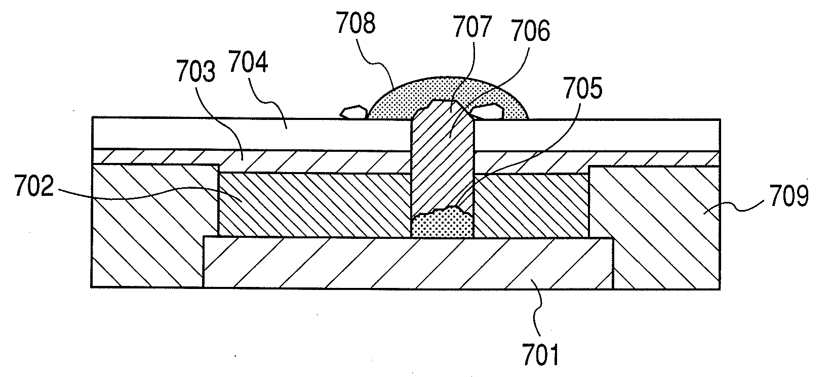
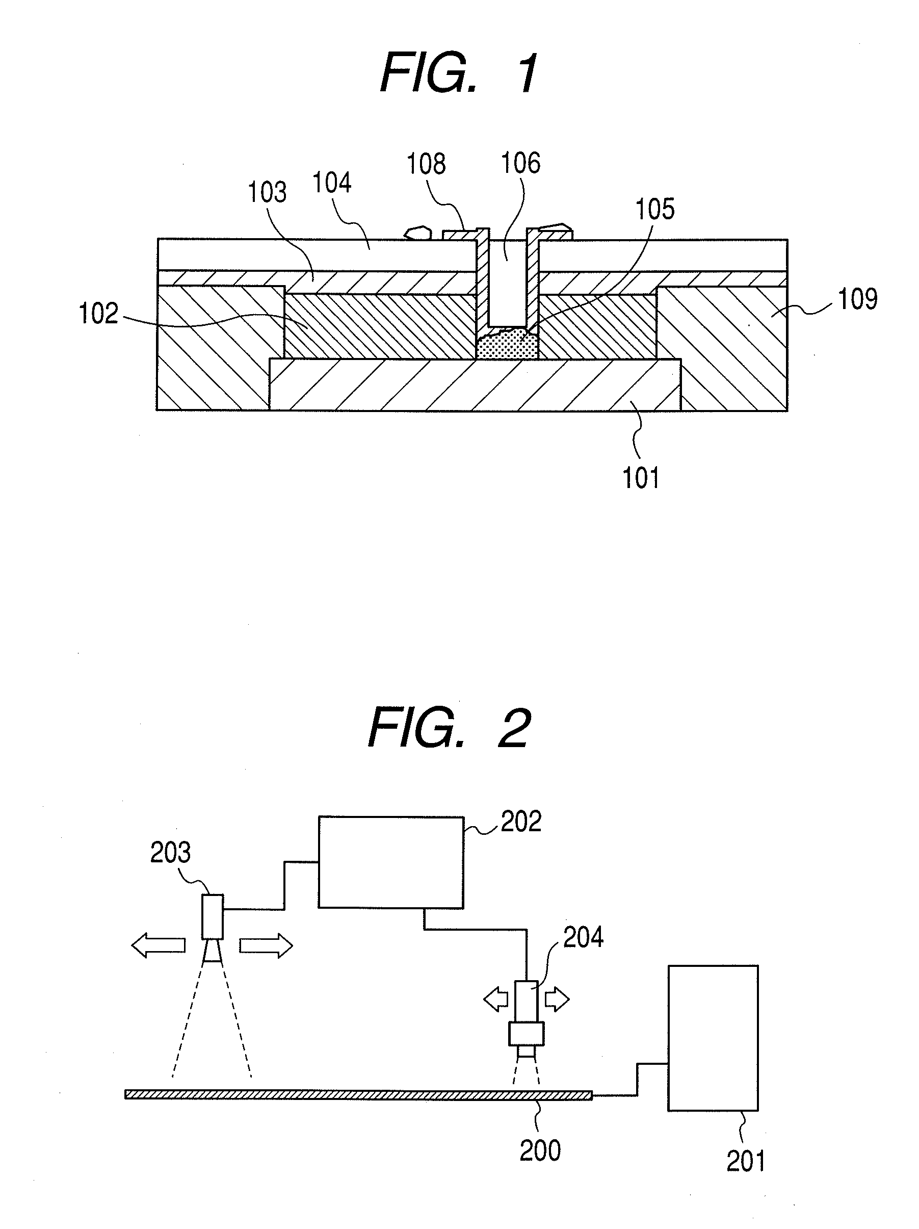
[0059]FIG. 5 schematically shows an organic light emitting device before a short-circuited site is repaired. A plurality of organic light emitting devices shown in FIG. 5 are formed on a substrate, and in this Example, a short-circuited site among a plurality of organic light emitting devices is repaired in the following process. In FIG. 5, 501 denotes a first electrode, 502 denotes an organic layer, 503 denotes a second electrode, 504 denotes a first sealing layer, 505 denotes a particle, 506 denotes a short-circuited site, and 509 denotes a device separating layer.

[0060]First, the organic layer 502 was vapor-deposited on an integrated substrate with a size of 400 mm×500 mm with a TFT circuit (not shown) and the first electrode 501 mounted thereon. On the substrate, a plurality of device patterns are placed separately, and are separated after the completion of the production of organic light emitting devices.

[0061]In each device pattern...

example 2

[0075]An organic layer was vapor-deposited, and a second electrode and a first sealing layer were formed thereon successively, using a substrate similar to that produced in Example 1.

[0076]Next, each pixel was subjected to alignment correction, and thereafter, a light emission inspection was performed, whereby a short-circuited site was removed with a laser in the same way as in Example 1 except for setting the wavelength of a laser to be 266 nm.

[0077]Next, the short-circuited site which has been removed was filled with an insulating member. A hole injection material dissolved in an organic solvent was used as a filling material. At this time, the organic light emitting device with the first sealing layer formed thereon was kept at 60° C., and the organic solvent was evaporated immediately after being injected onto a substrate. The short-circuited site which has been removed was filled with a solution in which 0.5% triphenylamine was dissolved as a hole injection material with an in...


PUM


Abstract

The present invention provides a method of producing an organic light emitting device capable of repairing a short-circuit between electrodes. The method includes: forming an organic light emitting device including a first electrode, an organic light emitting layer, and a second electrode successively on a substrate, and forming a first sealing layer on the second electrode; removing a short-circuited site of the organic light emitting device by irradiating at least the first sealing layer and the second electrode with a laser in the short-circuited site of the organic light emitting device; and forming a second sealing layer in the short-circuited site which has been removed.

Description

BACKGROUND OF THE INVENTION[0001]1. Field of the Invention[0002]The present invention relates to a method of producing an organic light emitting device (organic electroluminescence device) used for a display, a light source, or an illumination, and more particularly, to a method of repairing a short-circuited site of the organic light emitting device.[0003]2. Description of the Related Art[0004]Recently, in the development of an organic light emitting device (hereinafter, sometimes abbreviated simply as device), an attempt has been made so as to enhance the characteristics of the device. The organic light emitting device is a light-weight self light emitting device, so an apparatus using an organic light emitting device as a display pixel is expected as a next-generation display apparatus. However, for some reasons, when a part of an organic layer between a first electrode and a second electrode is not formed, and the electrodes are short-circuited, pixels (devices) will become non-...

Claims


Application Information

Patent Timeline
Patent Type & Authority Applications(United States)
IPC IPC(8): H01J9/50
CPCH01L51/5237H01L2251/568H01L51/56H10K50/844H10K71/00H10K71/861
Inventor MATSUDA, KOICHI
Owner CANON KK
Why Eureka
Try Eureka