Structure and methods for stress concentrating spacer

Inactive Publication Date: 2008-10-02
IBM CORP
View PDF3 Cites 72 Cited by
  • Summary
  • Abstract
  • Description
  • Claims
  • Application Information

AI Technical Summary

Benefits of technology

[0008]The present invention addresses the needs described above by providing a metal-oxide-semiconductor field effect transistor (MOSFET) stru

Problems solved by technology

Since the band structure of the channel is entirely determined by the stress of the channel, but is independent of the stress on the gate electrode, the stress applied to the gate elect

Method used


Image

  • Structure and methods for stress concentrating spacer
  • Structure and methods for stress concentrating spacer
  • Structure and methods for stress concentrating spacer

Examples


Embodiment Construction

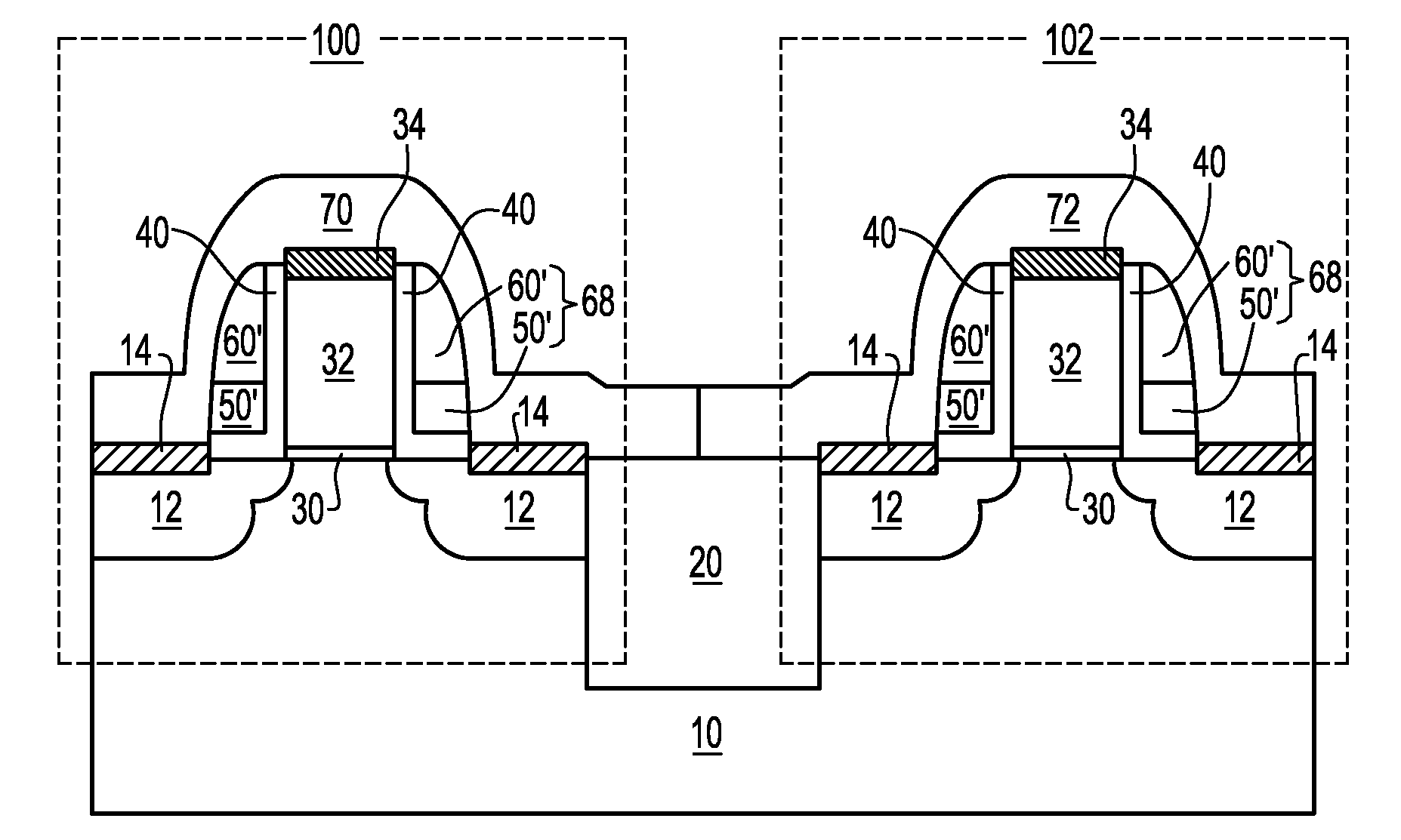
[0047]As stated above, the present invention relates to semiconductor structures that concentrate liner stress on a channel of a metal-oxide-semiconductor field effect transistor (MOSFET) and methods of manufacturing the same, which are now described in detail with accompanying figures. It is noted that like and corresponding elements are referred to by like reference numerals.

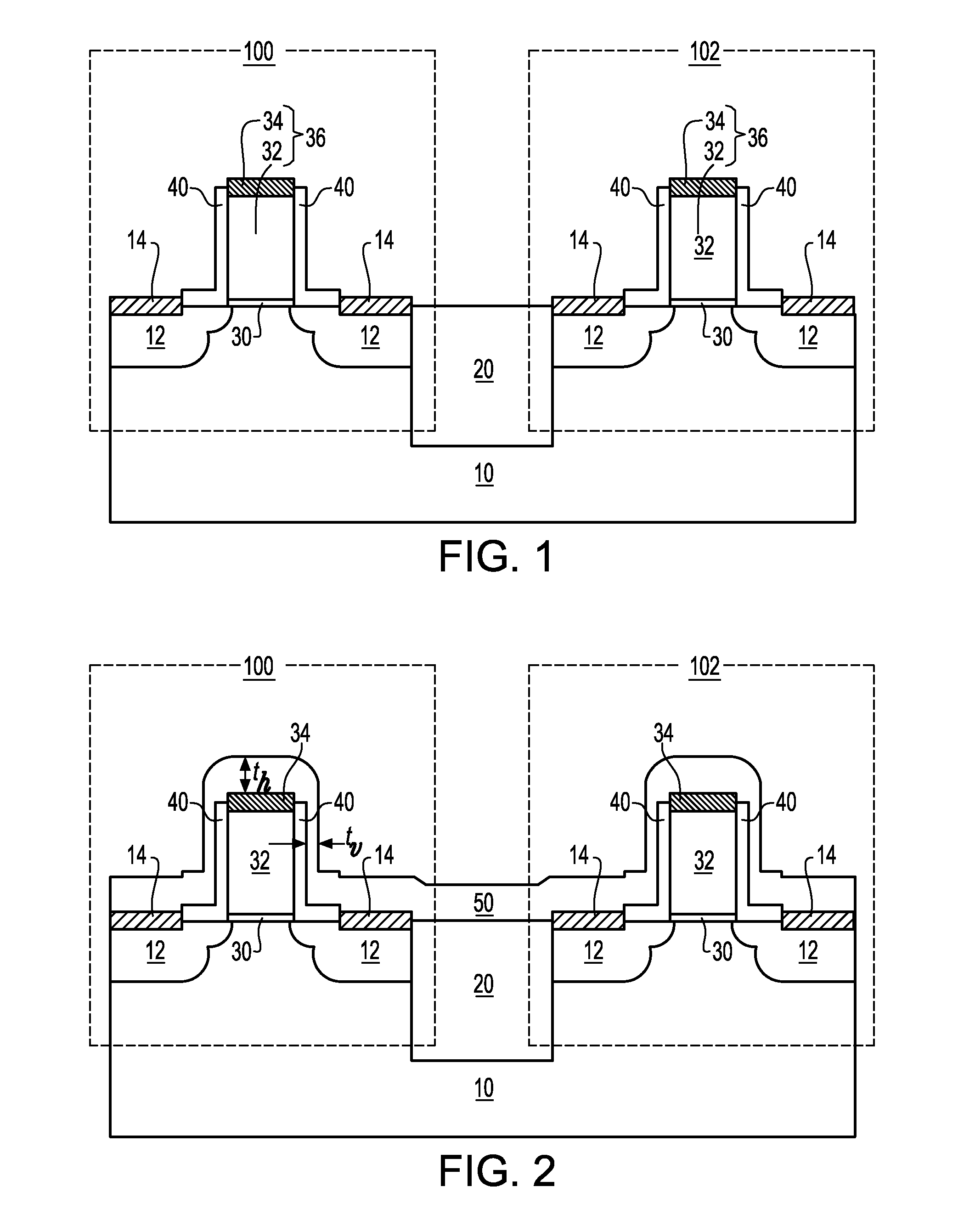
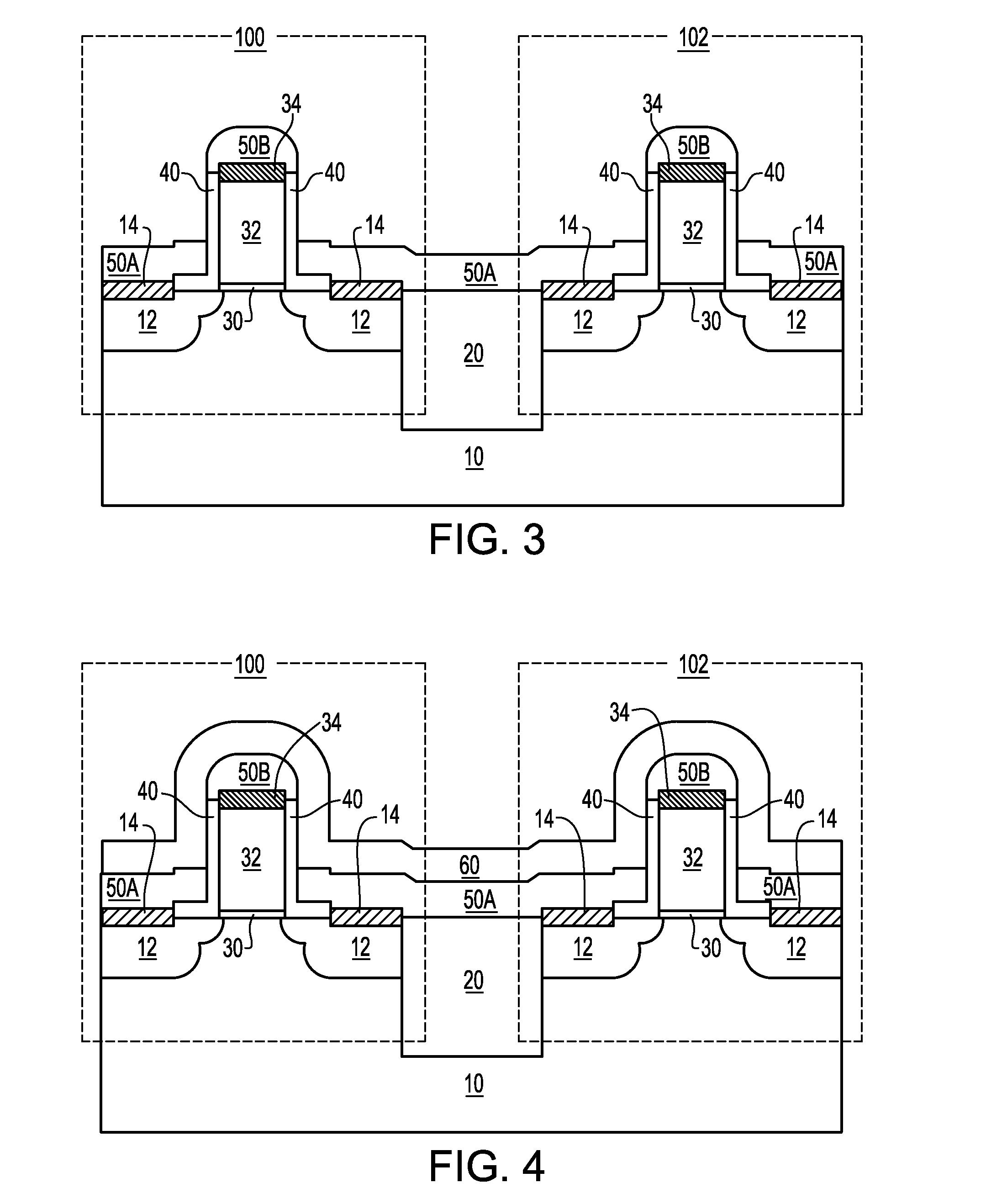
[0048]Referring to FIG. 1, a first exemplary structure according to the first embodiment is shown. The first exemplary structure comprises a p-type field effect transistor (PFET) 100 and an n-type field effect transistor (NFET) 102, each of which comprises a gate dielectric 30 formed on a semiconductor substrate 10, a gate semiconductor 32, a gate metal semiconductor alloy 34, an L-shaped inner gate spacer 40, source and drain regions 12 formed within the semiconductor substrate 10, and a source and drain metal semiconductor alloy 14 formed on the source and drain regions 12. The PFET 100 and the NFET 102 are ...


PUM


Abstract

A stress-concentrating spacer structure is a stack of an upper gate spacer with a low Young's modulus and a lower gate spacer with a high Young's modulus. The stacked spacer structure surrounds the gate electrode. The stress-concentrating spacer structure may contact an inner gate spacer that contacts the gate electrode or may directly contact the gate electrode. The upper gate spacer deforms substantially more than the lower gate spacer. The stress generated by the stress liner is thus transmitted primarily through the lower gate spacer to the gate electrode and subsequently to the channel of the MOSFET. The efficiency of the transmission of the stress from the stress liner to the channel is thus enhanced compared to conventional MOSFETs structure with a vertically uniform composition within a spacer.

Description

FIELD OF THE INVENTION[0001]The present invention relates to semiconductor structures with stress, and particularly to semiconductor structures that concentrate liner stress on a channel of a metal-oxide-semiconductor field effect transistor (MOSFET) and methods of manufacturing the same.BACKGROUND OF THE INVENTION[0002]A key metric for performance of transistors is the on-current, which is the current of a transistor per unit gate width when it is turned on. The on-current may be altered by changes in the band structure of the semiconductor substrate on which the transistor is formed. While the nature of stress needed to increase the on-current of a transistor may be dependent on the semiconductor substrate and the type of the transistor, in general, the band structure of a semiconductor device may be altered to increase the mobility of charge carriers, i.e., electrons or holes. For example, by manipulating transistor structures such that a favorable type of stress is applied to ea...

Claims


Application Information

Patent Timeline
IPC IPC(8): H01L27/092H01L21/8238
CPCH01L21/823807H01L21/823864H01L29/7843Y10S438/938
Inventor DYER, THOMAS W.
Owner IBM CORP
Why Eureka
Try Eureka