Terminal device, center device, optical communication network system and upstream signal timing control method

a technology of optical communication network system and upstream signal, applied in multi-channel communication, wavelength-division multiplex system, time-division optical multiplex system, etc., can solve the problems of complex software control, continuous scheduling, and cost of system construction

Inactive Publication Date: 2008-10-02
OKI ELECTRIC IND CO LTD
View PDF2 Cites 12 Cited by
  • Summary
  • Abstract
  • Description
  • Claims
  • Application Information

AI Technical Summary

Benefits of technology

[0015]The present invention has been made in view of the above circumstances and provides a terminal device, a center device, an optical communication network system and an upstream signal timing control method.
[0016]According to an aspect of the invention, there is provided an upstream signal timing control method which controls a timing of an upstream optical signal, from a terminal device to a center device, to a timing that the center device intends, the upstream signal timing control method comprising: transmitting, from the center device to the terminal device, optical clock pulses synchronized with the timing that the center device intends; the terminal device controlling a delay of th

Problems solved by technology

Moreover, in systems which employ dynamic bandwidth allocation, it is necessary to continually perform complex scheduling.
Consequently, the cost of system construction is an issue.
Furthermore, with the DBA algorithm employed in the technology described in the aforementioned “GE-PON technolo

Method used


Image

  • Terminal device, center device, optical communication network system and upstream signal timing control method
  • Terminal device, center device, optical communication network system and upstream signal timing control method
  • Terminal device, center device, optical communication network system and upstream signal timing control method

Examples


embodiment

Structure of Embodiment

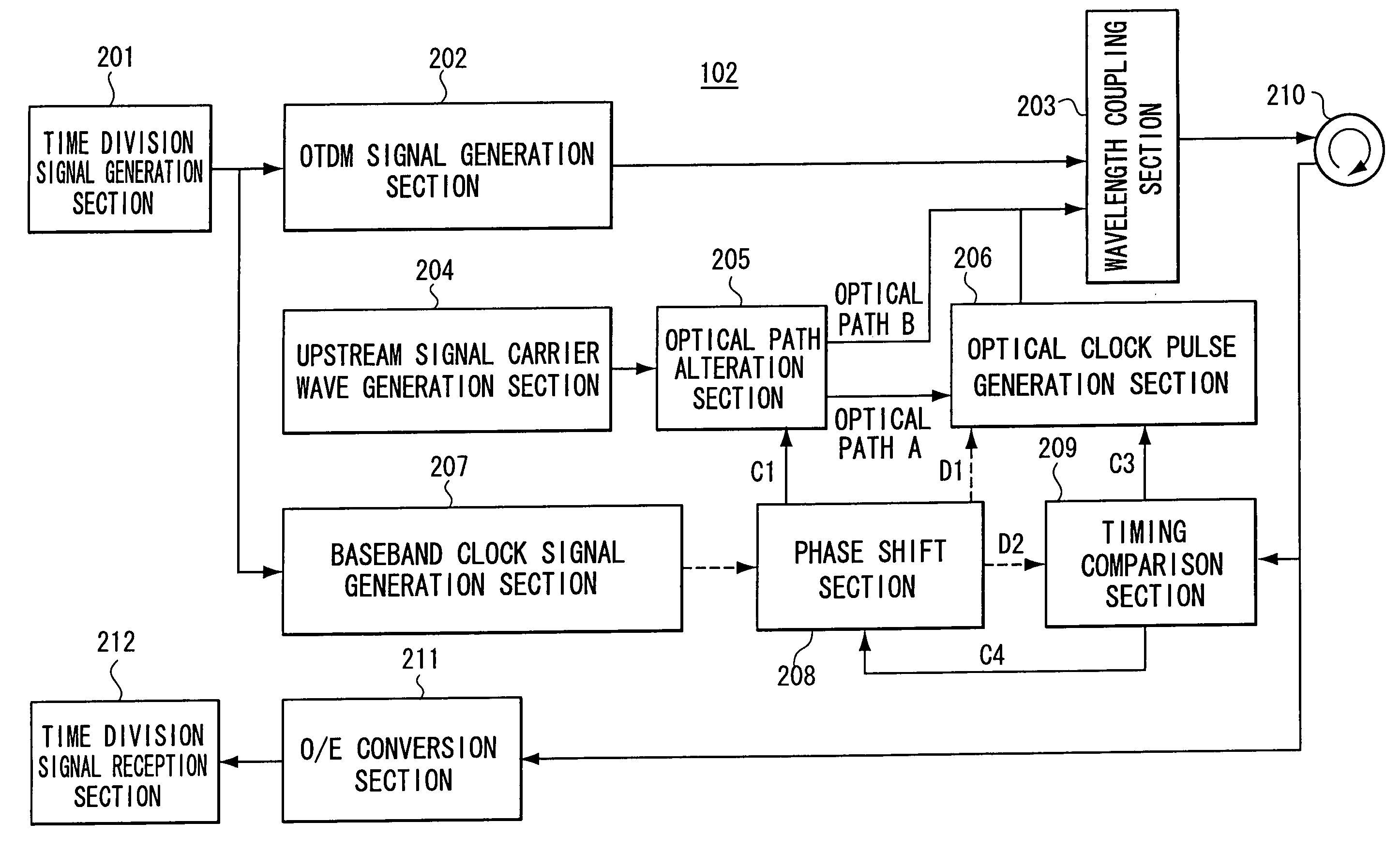
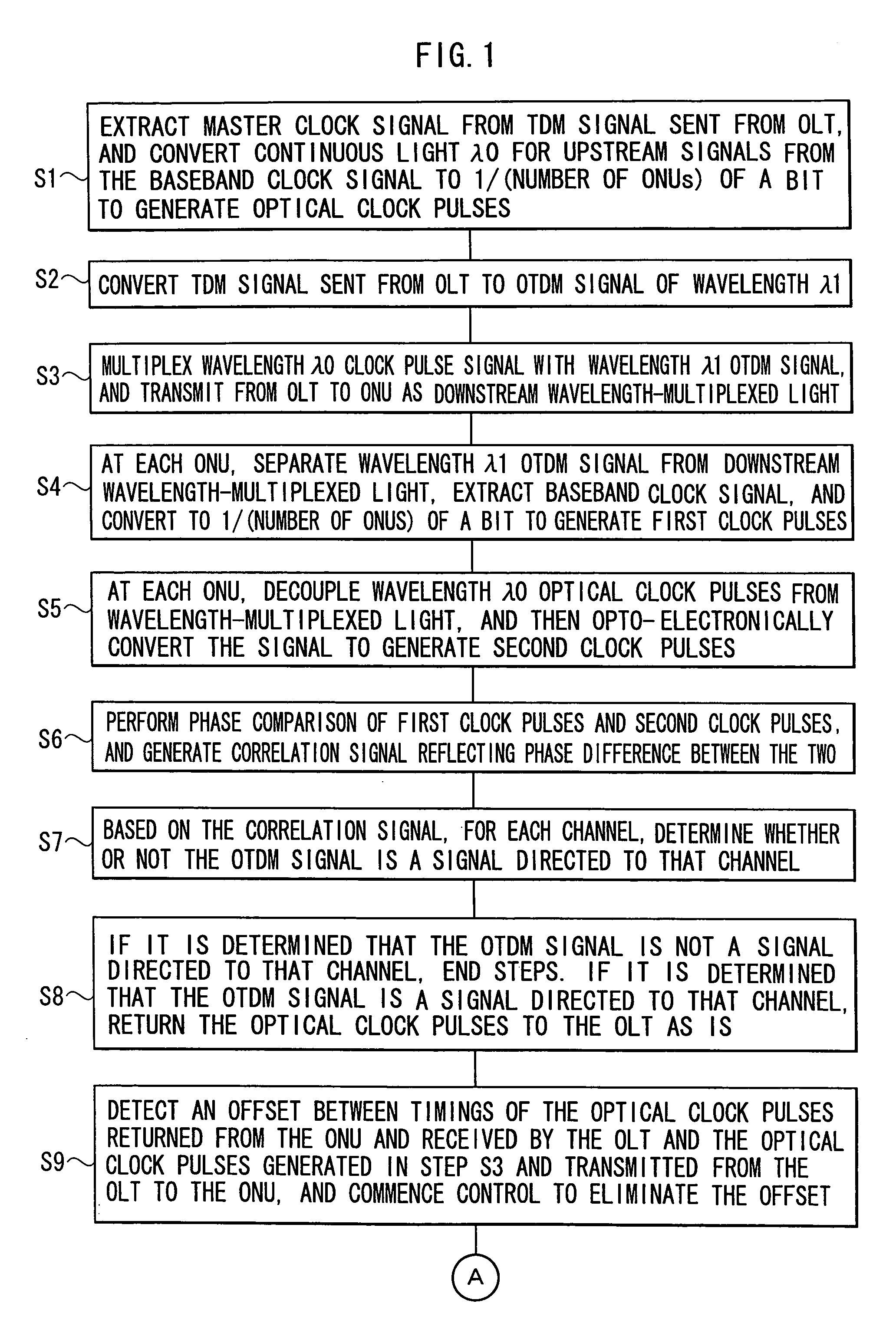
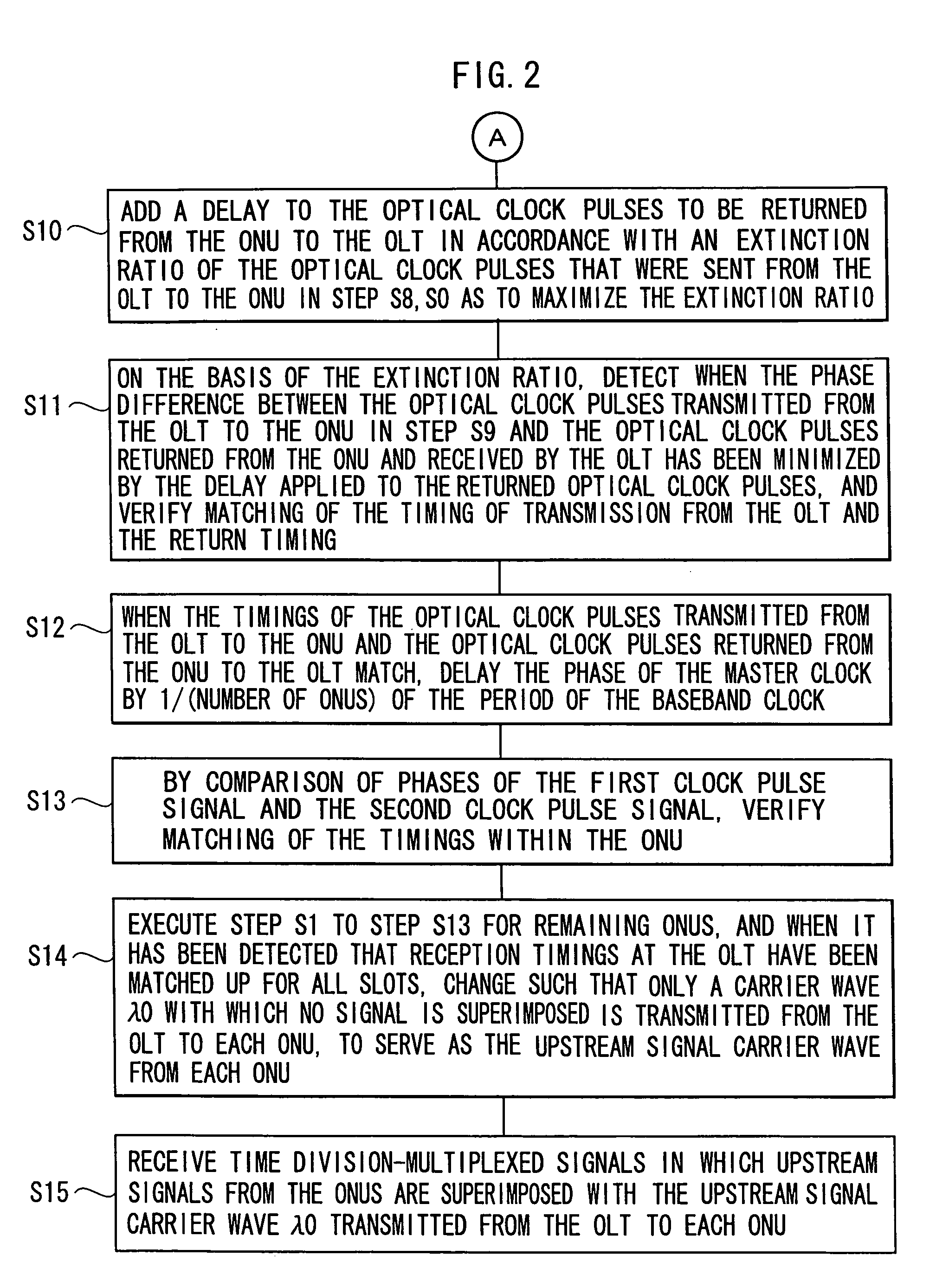
[0036]FIG. 3 is a block diagram showing basic structure of a bidirectional time division multiplexing optical communication network system of the embodiment.

[0037]In FIG. 3, a bidirectional time division multiplexing optical communication network system 100 of the embodiment is provided with a digital exchange 101 and an optical line terminal (OLT) 102 which serve as a office side structure, is provided with a plurality (four are shown in FIG. 3, but four is not a limitation) of optical network units (ONU) 104-1 to 104-4 which serve as subscriber side structures, and includes an optical splitter (optical branch circuit) 103. The OLT 102 and optical splitter 103 are connected together by a single optical fiber (optical fiber propagation path) 105. The ONUs 104-1 to 104-4 are connected with the optical splitter 103 by single optical fibers 106-1 to 106-4, respectively. Considering portions of a network that implements optical communications, the OLT 102 correspo...


PUM


Abstract

An upstream signal timing control method which controls a timing of an upstream optical signal, from a terminal device to a center device, to a timing that the center device intends. Optical clock pulses synchronized with the timing that the center device intends are sent from the center device to the terminal device. The terminal device delay-controls the optical clock pulses and retransmits them to the center device. The center device detects an offset between the timing and a timing of the returned optical clock pulses, and applies timing offset information to the transmitted optical clock pulses. The terminal device performs the delay control in accordance with the timing offset information applied to the received optical clock pulses. When the offset between the timing and the returned optical clock pulse timing is at or below a threshold, the center device verifies completion of timing control of the upstream optical signal.

Description

CROSS-REFERENCE TO RELATED APPLICATION[0001]This application claims priority under 35 USC 119 from Japanese Patent Application No. 2007-079827, the disclosure of which is incorporated by reference herein.BACKGROUND OF THE INVENTION[0002]1. Field of the Invention[0003]The present invention relates to a terminal device, a center device, an optical communication network system and an upstream signal timing control method. The present invention is applicable to, for example, a bidirectional time division multiplexing optical communication network system, for performing bidirectional communications using time division multiplexing (TDM) between a center (central office) device and a number of terminal devices with a PON (passive optical network). In particular, the present invention is applicable to a time slot control method for establishing synchronization of upstream signals from the terminal devices to the center device, and a structure for implementing the control method.[0004]2. De...

Claims


Application Information

Patent Timeline
IPC IPC(8): H04J14/08H04B10/00H04B10/07H04B10/272H04B10/524H04J14/00H04J14/02
CPCH04J14/0282H04J14/08
Inventor FUJII, AKIHIRO
Owner OKI ELECTRIC IND CO LTD
Why Eureka
Try Eureka