
Atomic layer deposition reactor

a technology of atomic layer and reactor, which is applied in the direction of coating, electric discharge tube, metal material coating process, etc., can solve the problems of contaminating the film, preventing the use of higher pressure, and arcing in the chamber

Inactive Publication Date: 2008-10-02
ASM INTERNATIONAL
View PDF92 Cites 355 Cited by
  • Summary
  • Abstract
  • Description
  • Claims
  • Application Information

AI Technical Summary

Problems solved by technology

Few precursors, however, exhibit this idealized behavior due to time-dependent adsorption-desorption phenomena, blocking of the primary reaction by-products of the primary reaction, total consumption of the second precursor in the upstream-part of the reactor chamber, uneven adsorption / desorption of the first precursor due to uneven flow conditions in the reaction chamber, or any of various other possible factors.
However, this method can result in sputtering by the plasma, which may contaminate the film as sputtered materials from parts in the reaction chamber contact the substrate.
Yet another disadvantage is that, when depositing conducting materials, arcing in the chamber can occur because the insulators used to isolate the RF from ground can also become coated with the deposited conducting material.
However, remote radical generation techniques should provide sufficient radical densities at the substrate surface, notwithstanding the significant losses that can occur on transport of the radical to the reaction chamber.
Radical losses are generally severe at higher pressure (>10 torr), thus precluding the use of higher pressure to separate the reactants in an ALD process.
In addition, the distribution of radicals is typically non-uniform.

Method used


Image

  • Atomic layer deposition reactor
  • Atomic layer deposition reactor
  • Atomic layer deposition reactor

Examples


Embodiment Construction

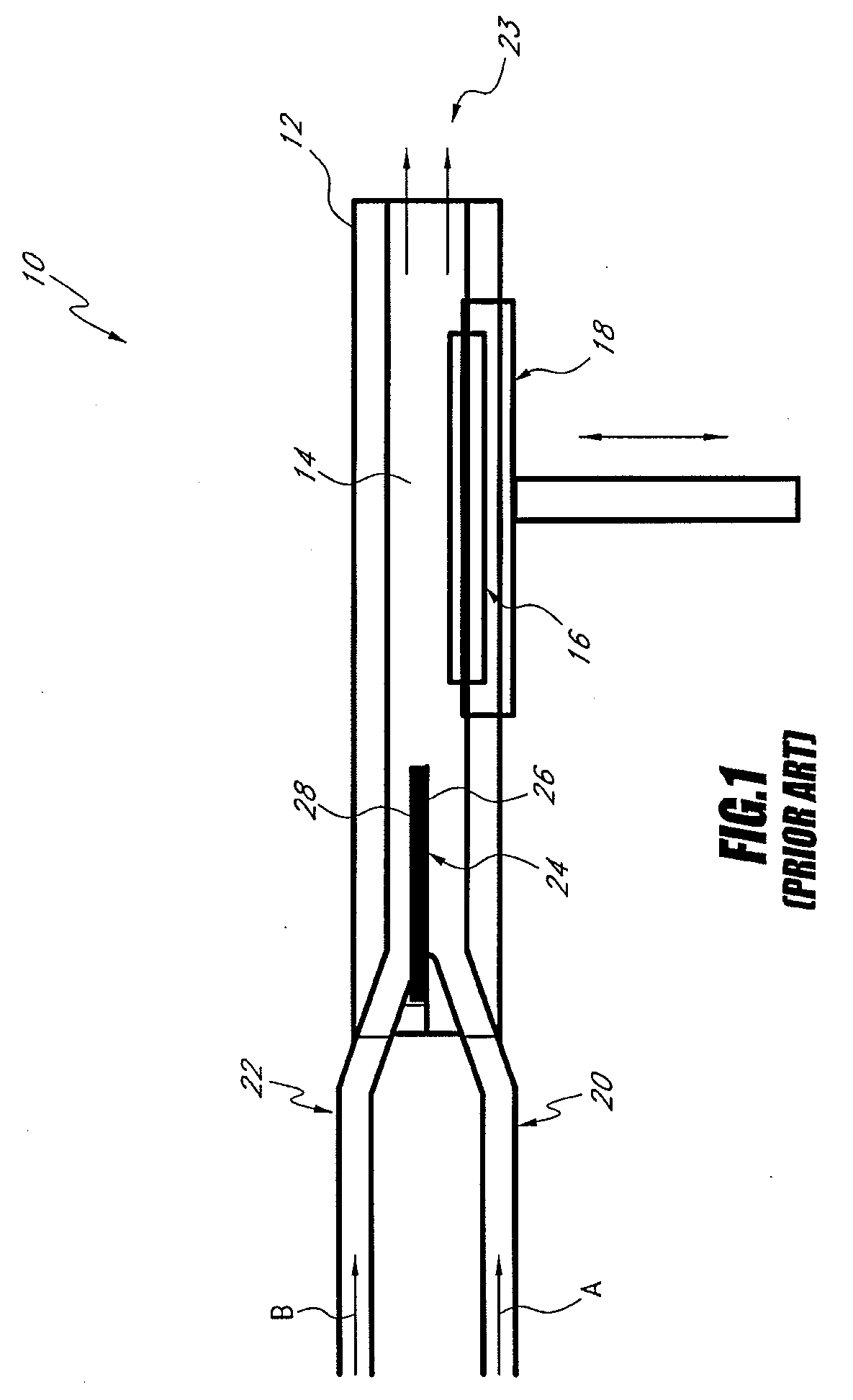
[0041]FIG. 1 schematically illustrates an exemplary prior art ALD reactor 10. The reactor 10 includes a reactor chamber 12, which defines, at least in part, a reaction space 14. A wafer or substrate 16 is disposed within the reaction chamber 14 and is supported by a pedestal 18. The pedestal 18 is configured to move the wafer 16 in and out of the reaction chamber 14. In other arrangements, the reactor can include an inlet / outlet port and an external robot with a robotic arm for wafer transfer. The robot arm can be configured to (i) move the substrate into the reactor through the inlet / outlet port, (ii) place the substrate on the pedestal, (iii) lift the substrate from the pedestal and / or (iv) remove the substrate from the reactor through the inlet / outlet port.

[0042]In the illustrated reactor 10, two ALD reactants or precursors, A and B, are supplied to the reaction space 14. The first reactant or precursor A is supplied to the reaction chamber 14 through a first supply conduit 20. I...


PUM

PropertyMeasurementUnit
widthaaaaaaaaaa
widthaaaaaaaaaa
pressureaaaaaaaaaa

Abstract

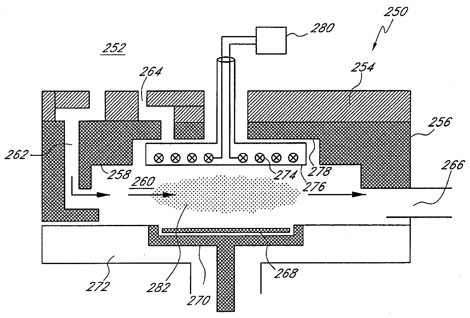
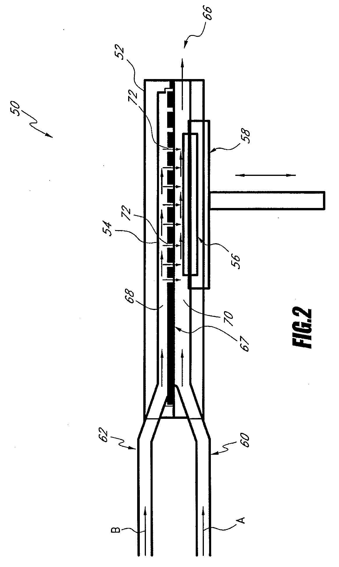
Various reactors for growing thin films on a substrate by subjecting the substrate to alternately repeated surface reactions of vapor-phase reactants are disclosed. The reactor according to the present invention includes a reaction chamber, a substrate holder, a showerhead plate, a first reactant source, a remote radical generator, a second reactant source, and an exhaust outlet. The showerhead plate is configured to define a reaction space between the showerhead plate and the substrate holder. The showerhead plate includes a plurality of passages leading into the reaction space. The substrate is disposed within the reaction space. A first non-radical reactant is supplied through the showerhead plate to the reaction space. The remote radical generator produces the radicals of a second reactant supplied from the second reactant source. The radicals are supplied directly to the reaction space without passing through the showerhead plate.

Description

RELATED PATENTS AND APPLICATIONS[0001]This application is related to U.S. Pat. No. 6,820,570, filed Aug. 14, 2002 and granted Nov. 23, 2004 (attorney docket No. ASMMC.037AUS); U.S. patent application Ser. No. 10 / 991,556, filed Nov. 18, 2004 (attorney docket No. ASMMC.037C1); U.S. Pat. No. 6,511,539, filed Sep. 8, 1999 and granted Jan. 28, 2003 (attorney docket No. ASMMC.001AUS); and U.S. patent application Ser. No. 10 / 317,266, filed Dec. 10, 2002 (attorney docket No. ASMMC.001DV1), the entire contents of these applications are hereby incorporated by reference herein.BACKGROUND OF THE INVENTION[0002]1. Field of the Invention[0003]The present invention relates to an apparatus for growing thin films on a surface of a substrate. More particularly, the present invention relates to an apparatus for producing thin films on the surface of a substrate by subjecting the substrate to alternately repeated surface reactions of vapor-phase reactants.[0004]2. Description of the Related Art[0005]Th...

Claims


Application Information

Patent Timeline
Patent Type & Authority Applications(United States)
IPC IPC(8): C23C16/00
CPCC23C16/452C23C16/45536C23C16/45565H01J37/3244C23C16/45544
Inventor KETO, LEIF R.
Owner ASM INTERNATIONAL
Learn More