Pixel structure and method for forming the same

Active Publication Date: 2008-10-09
AU OPTRONICS CORP
View PDF11 Cites 27 Cited by
  • Summary
  • Abstract
  • Description
  • Claims
  • Application Information

AI Technical Summary

Benefits of technology

[0009]The present invention is directed to a pixel structure and a method for forming the same is ad

Problems solved by technology

Such problem arises more often in a panel o

Method used


Image

  • Pixel structure and method for forming the same
  • Pixel structure and method for forming the same
  • Pixel structure and method for forming the same

Examples


first embodiment

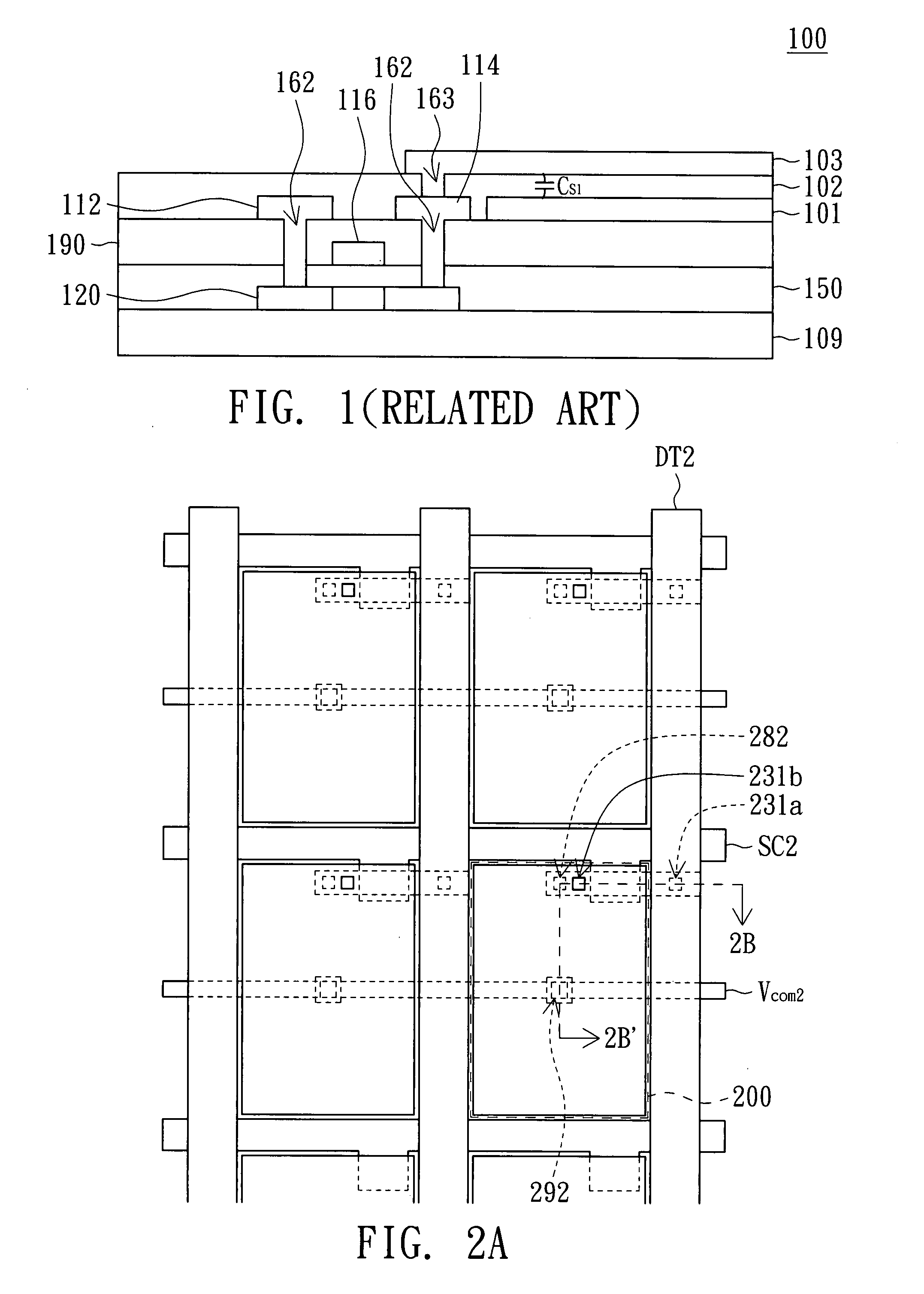
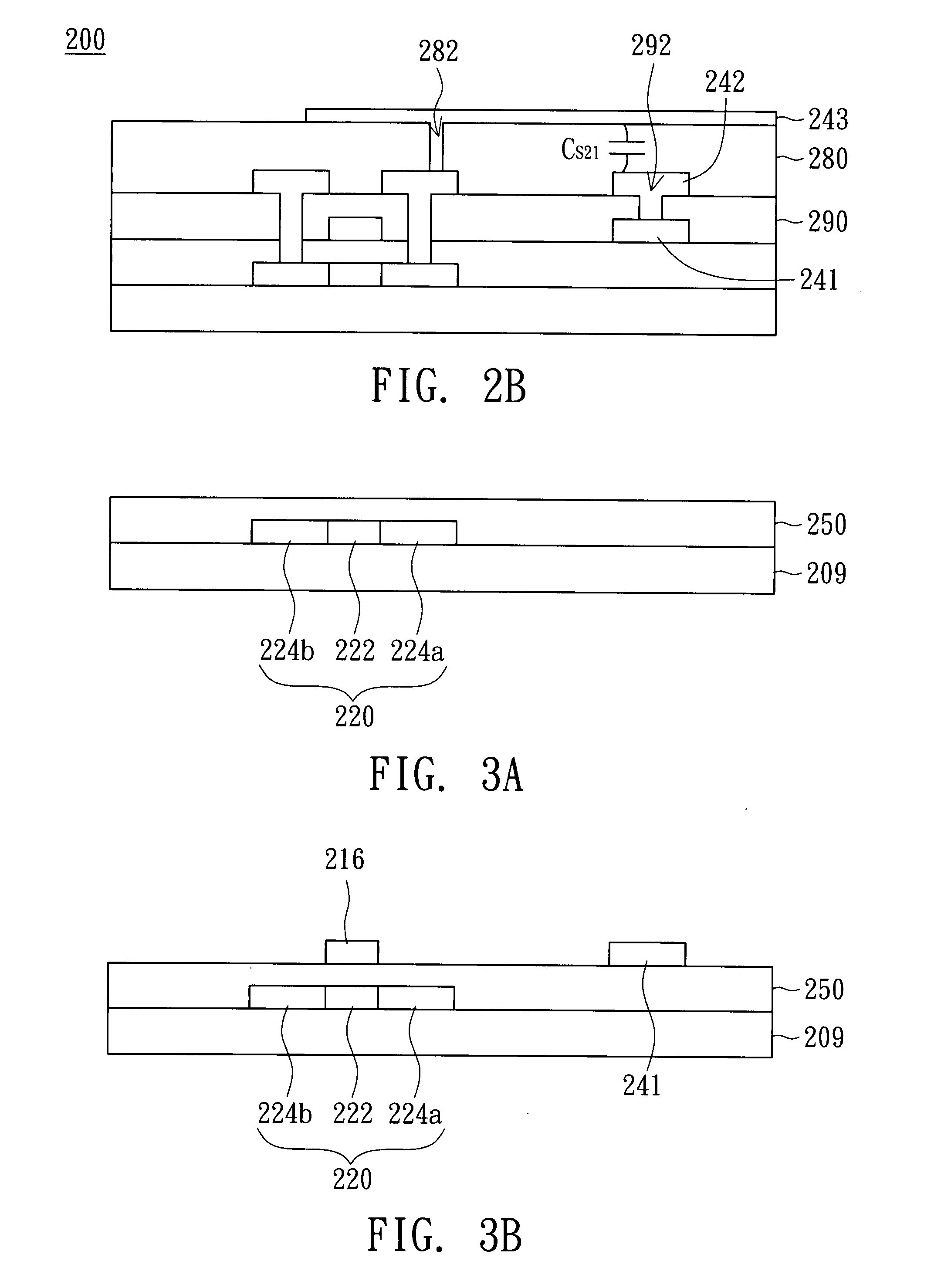
[0030]Referring to FIG. 2A, a top view of a pixel structure according to a first embodiment of the present invention is shown. The present embodiment of the invention is exemplified by a pixel structure 200 of a display panel of an electro-optical device. As indicated in FIG. 2A, a data line DT2 and a scan line SC2 are electrically connected to the pixel structure 200, respectively. Referring to FIG. 2B, a cross-sectional view of the pixel structure of FIG. 2A is shown. FIG. 2B is a cross-sectional view along the cross-sectional line 2B-2B′ of FIG. 2A. The pixel structure 200 comprises a transistor (not numbered in the diagram), a first storage capacitor Cs21, a first conductive layer 241, an interlayer dielectric layer 290, a second conductive layer 242, a passivation layer 280, and a third conductive layer 243. Preferably, the pixel structure 200 selectively comprises a light-shading patterned layer (not illustrated in the diagram) located and substantially paralleled a side of at...

second embodiment

[0041]Referring to FIG. 5A, a top view of a pixel structure according to a second embodiment of the present invention is shown. The present embodiment of the invention is exemplified by a pixel structure 400 of a display panel of an electro-optical device. As indicated in FIG. 5A, data lines DT41 and DT42 and a scan line SC4 are electrically connected to the pixel structure 400, respectively. Referring to FIG. 5B, a cross-sectional view of the pixel structure of FIG. 5A is shown. FIG. 5B is a cross-sectional view along the cross-sectional line 5B-5B′ of FIG. 5A. The pixel structure 400 comprises a transistor (not numbered in the diagram), a first storage capacitor Cs41, a first conductive layer 441, an interlayer dielectric layer 490, a second conductive layer 442, a passivation layer 480, a third conductive layer 443, and a fourth conductive layer 444. Preferably, the pixel structure 400 selectively comprises a light-shading patterned layer (not illustrated in the diagram) located ...

third embodiment

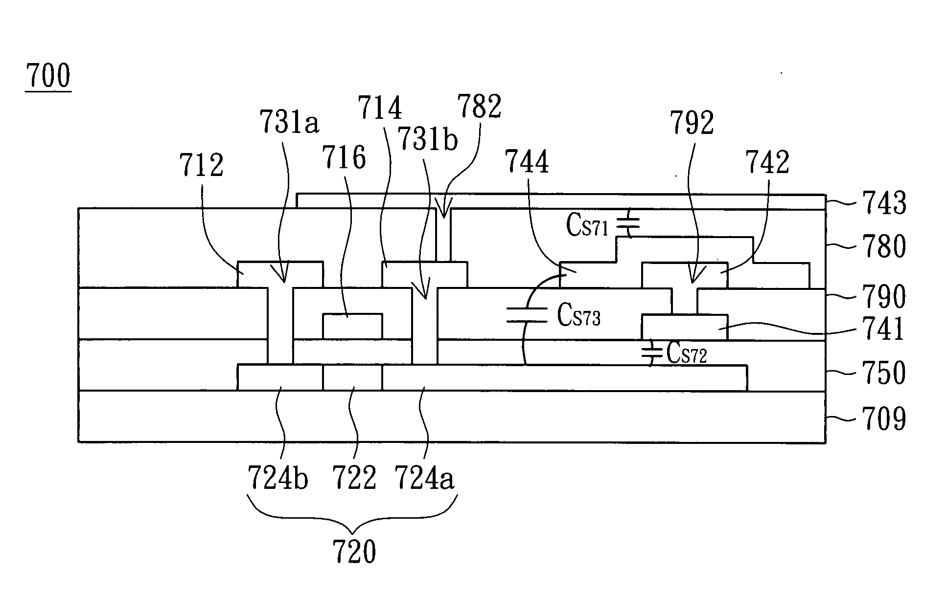
[0054]Referring to FIG. 7A, a top view of a pixel structure according to a third embodiment of the present invention is shown. The present embodiment of the invention is exemplified by a pixel structure 500 of a display panel of an electro-optical device. As indicated in FIG. 7A, a data line DT5 line DT5 and a scan line SC5 are electrically connected to the pixel structure 500, respectively. Referring to FIG. 7B, a cross-sectional view of the pixel structure of FIG. 7A is shown. FIG. 7B is a cross-sectional view along the cross-sectional line 7B-7B′ of FIG. 7A. The pixel structure 500 comprises a transistor (not numbered in the diagram), a first storage capacitor Cs51, a second storage capacitor Cs52, a third storage capacitor Cs53, a first conductive layer 541, an interlayer dielectric layer 590, a second conductive layer 542, an insulating layer 550, a semiconductor layer 520, a passivation layer 580, and a third conductive layer 543. Preferably, the pixel structure 500 selectivel...


PUM


Abstract

A pixel structure comprising at least one transistor, a first storage capacitor, a first conductive layer, an interlayer dielectric layer, a second conductive layer, a passivation layer, and a third conductive layer is provided. The first storage capacitor is electrically connected to the transistor. The interlayer dielectric layer having at least one first opening covers the first conductive layer. The second conductive layer is formed on a part of the interlayer dielectric layer and is electrically connected to the first conductive layer through the first opening. The passivation layer having at least one second opening covers the transistor and the second conductive layer. The third conductive layer is formed on a part of the passivation layer and is electrically connected to the transistor through the second opening. The first storage capacitor is formed by the third conductive layer, the passivation layer, and the second conductive layer.

Description

[0001]This application claims the benefit of priority based on Taiwan Application Number 96111888, filed Apr. 3, 2007, the subject matter of which is incorporated herein by reference in its entirety.BACKGROUND OF THE INVENTION[0002]1. Field of the Invention[0003]The present invention relates in general to a pixel structure and a method for forming the same, and more particularly, to a pixel structure having a storage capacitor.[0004]2. Description of the Related Art[0005]Referring to FIG. 1, a cross-sectional view of a conventional pixel structure is shown. The pixel structure 100 has a substrate 109 which has a semiconductor layer 120 formed thereon. The semiconductor layer 120 and the substrate 109 are covered by an insulating layer 150. The insulating layer 150 has a gate electrode 116 formed thereon and covered by an interlayer dielectric layer 190. The insulating layer 150 and the interlayer dielectric layer 190 have two openings 162 for exposing the semiconductor layer 120. A ...

Claims


Application Information

Patent Timeline
IPC IPC(8): H01L33/00H01L21/441
CPCG02F1/136213G02F1/136227H01L27/124H01L27/1255H01L27/3265H10K59/1216
Inventor TING, YU-HSIN
Owner AU OPTRONICS CORP
Why Eureka
Try Eureka