Apparatus of memory array using finfets

a technology of finfets and apparatuses, applied in electrical apparatus, semiconductor devices, semiconductor/solid-state device details, etc., can solve the problem of reducing the size of the switching device of logic circuits

Active Publication Date: 2008-10-16
INFINEON TECH AG
View PDF11 Cites 170 Cited by
  • Summary
  • Abstract
  • Description
  • Claims
  • Application Information

AI Technical Summary

Problems solved by technology

Additionally, the increasing demand of high density of logic circuitries also cau

Method used


Image

  • Apparatus of memory array using finfets
  • Apparatus of memory array using finfets
  • Apparatus of memory array using finfets

Examples


Embodiment Construction

[0007]In the following description, for purposes of explanation, numerous specific details are set forth in order to provide a thorough understanding of example embodiments. It will be evident, however, to one skilled in the art that the embodiments of the invention may be practiced without these specific details.

[0008]The term “FinFET” used in the following description denotes a type of multi-gate field effect transistor, i.e. MuGFET having a fin of material that functions as a channel for the transistor. The term “NVM” denotes a non-volatile memory. The term “PCRAM” denotes “a phase change random access memory”. The term “MRAM” denotes “a magnetic random access memory”. The term “CBRAM” denotes” a “conductive bridging random access memory. The term “FeRAM” denotes “ferroelectric random access memory”.

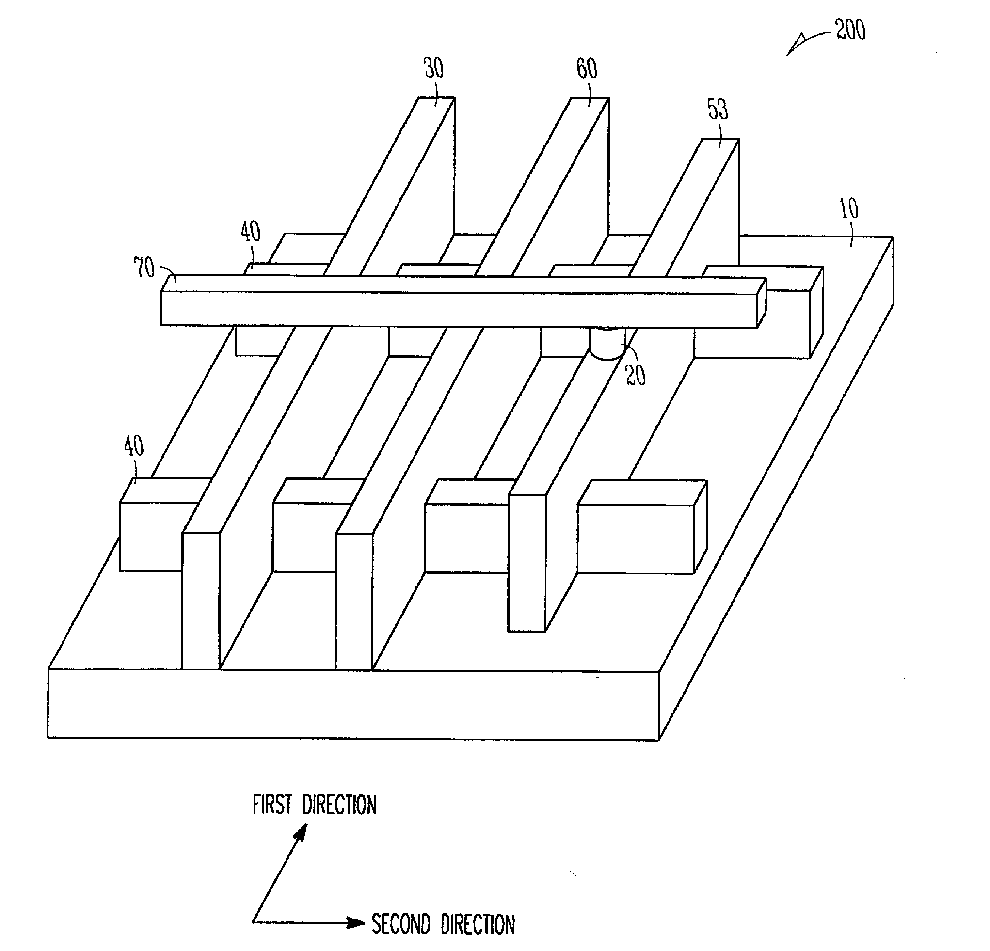
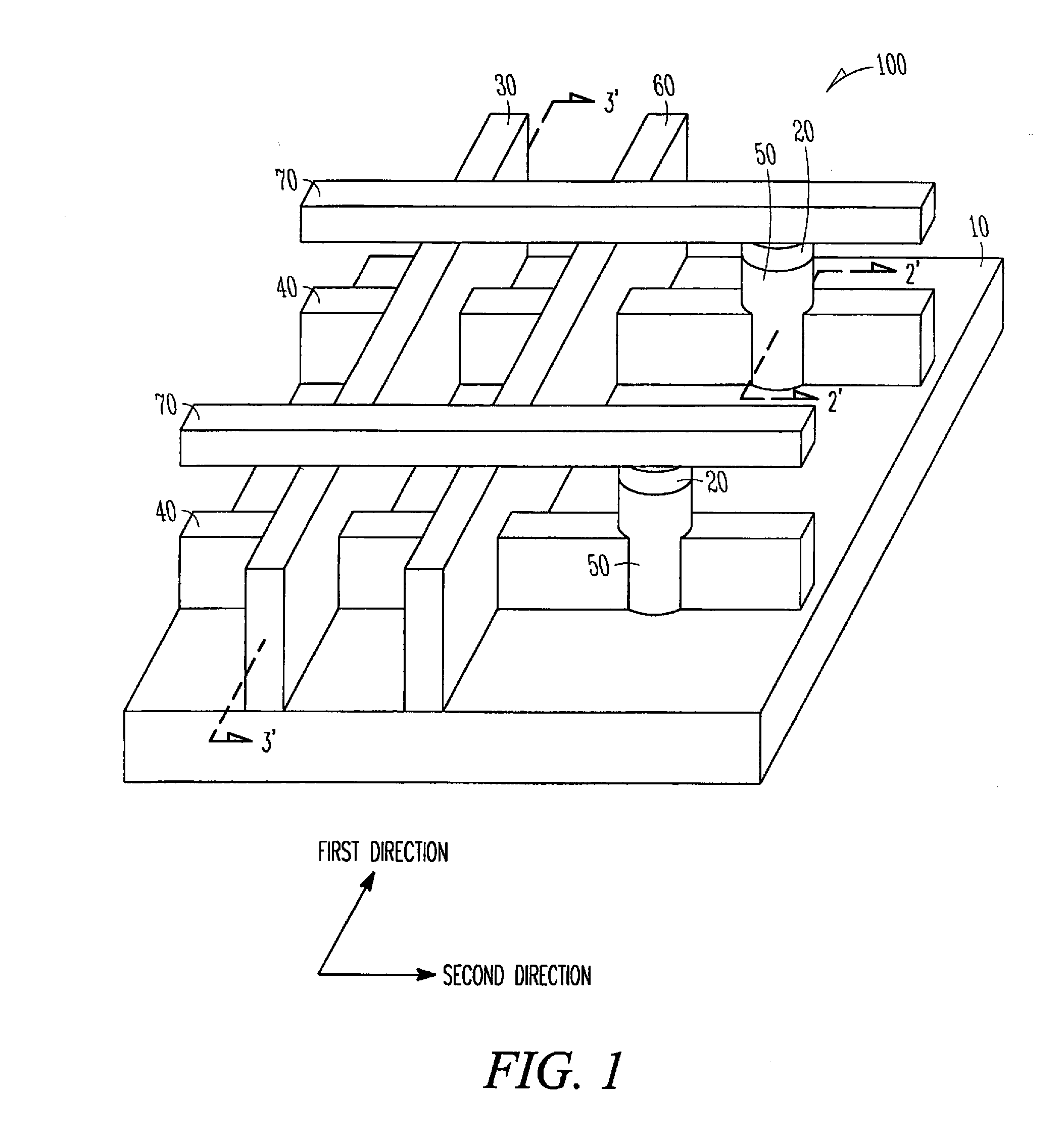
[0009]FIG. 1 is a perspective view of a portion of a memory cell array showing two cells, each with a FinFET select device and having bit line contacts in accordance with an embodimen...


PUM


Abstract

A memory cell includes a FinFET select device and a memory element. In some embodiments a memory cell has a contact element coupled between a surface of the fin and the memory element.

Description

TECHNICAL FIELD[0001]The various embodiments described herein relate generally to apparatus having memory cell arrays, and more particularly, to apparatus having memory cell arrays using FinFETs as select devices.BACKGROUND[0002]In recent years, with the increasing demand of high density of arrays of non-volatile memory (NVM) cells, e.g., phase change random access memories (PCRAM) and magnetic random access memories (MRAM), there is a significant need to reduce the size of the select devices of the NVM cells. Additionally, the increasing demand of high density of logic circuitries also causes the need to reduce the size of the switching devices of the logic circuitries.BRIEF DESCRIPTION OF THE DRAWINGS[0003]FIG. 1 is a perspective view of a unit of a memory cell array having a FinFET with a pair of bit line contacts, in accordance with an embodiment of the application;[0004]FIG. 2 is a cross-section view of the unit of the memory cell array shown in FIG. 1 through one of the bit li...

Claims


Application Information

Patent Timeline
IPC IPC(8): H01L31/0272H01L23/48H01L29/18
CPCH01L21/84H01L27/115H01L27/228H01L27/2436H01L27/2463H01L27/1052H01L45/04H01L45/06H01L45/085H01L45/1233H01L45/141H01L29/785H01L29/41791H10B63/30H10B61/22H10B63/80H10N70/231H10N70/245H10N70/826H10B69/00H10B99/00H10N70/20H10N70/882
Inventor KAKOSCHKE, RONALDSCHRUEFER, KLAUS
Owner INFINEON TECH AG
Why Eureka
Try Eureka