Strain enhanced semiconductor devices and methods for their fabrication

a technology of enhanced semiconductor devices and semiconductors, applied in the direction of semiconductor devices, basic electric elements, electrical equipment, etc., can solve the problems of reducing channel resistance and relaxing strain, and negating the effect of channel resistance reduction

Active Publication Date: 2008-10-16
ADVANCED MICRO DEVICES INC
View PDF13 Cites 74 Cited by
  • Summary
  • Abstract
  • Description
  • Claims
  • Application Information

AI Technical Summary

Benefits of technology

[0005]In accordance with one embodiment a strain enhanced semiconductor device having a source region and a drain region separated by a strained channel region is provided. The device includes a gate electrode overlying the s

Problems solved by technology

Unfortunately, the formation of a metal silicide layer on the source and drain regions has the side effect of causing a relaxation of the strain on the channel region caused by the embedded m

Method used


Image

  • Strain enhanced semiconductor devices and methods for their fabrication
  • Strain enhanced semiconductor devices and methods for their fabrication
  • Strain enhanced semiconductor devices and methods for their fabrication

Examples


Embodiment Construction

[0011]The following detailed description is merely exemplary in nature and is not intended to limit the invention or the application and uses of the invention. Furthermore, there is no intention to be bound by any expressed or implied theory presented in the preceding technical field, background, brief summary or the following detailed description.

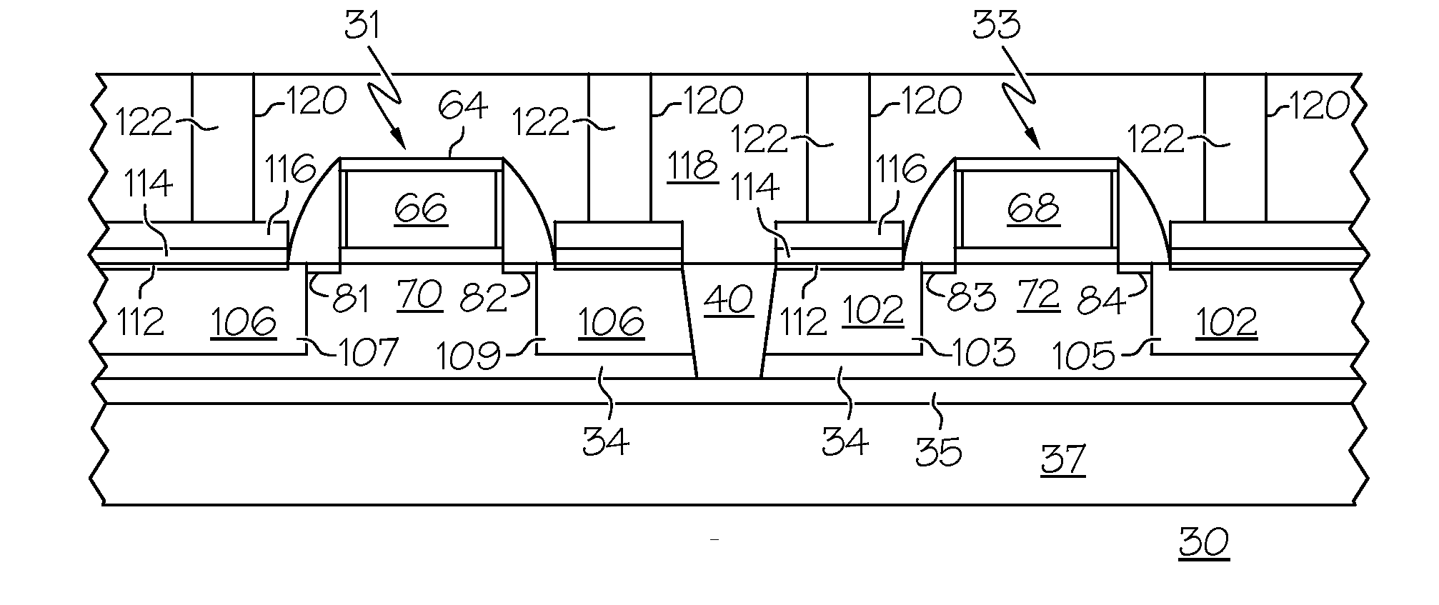
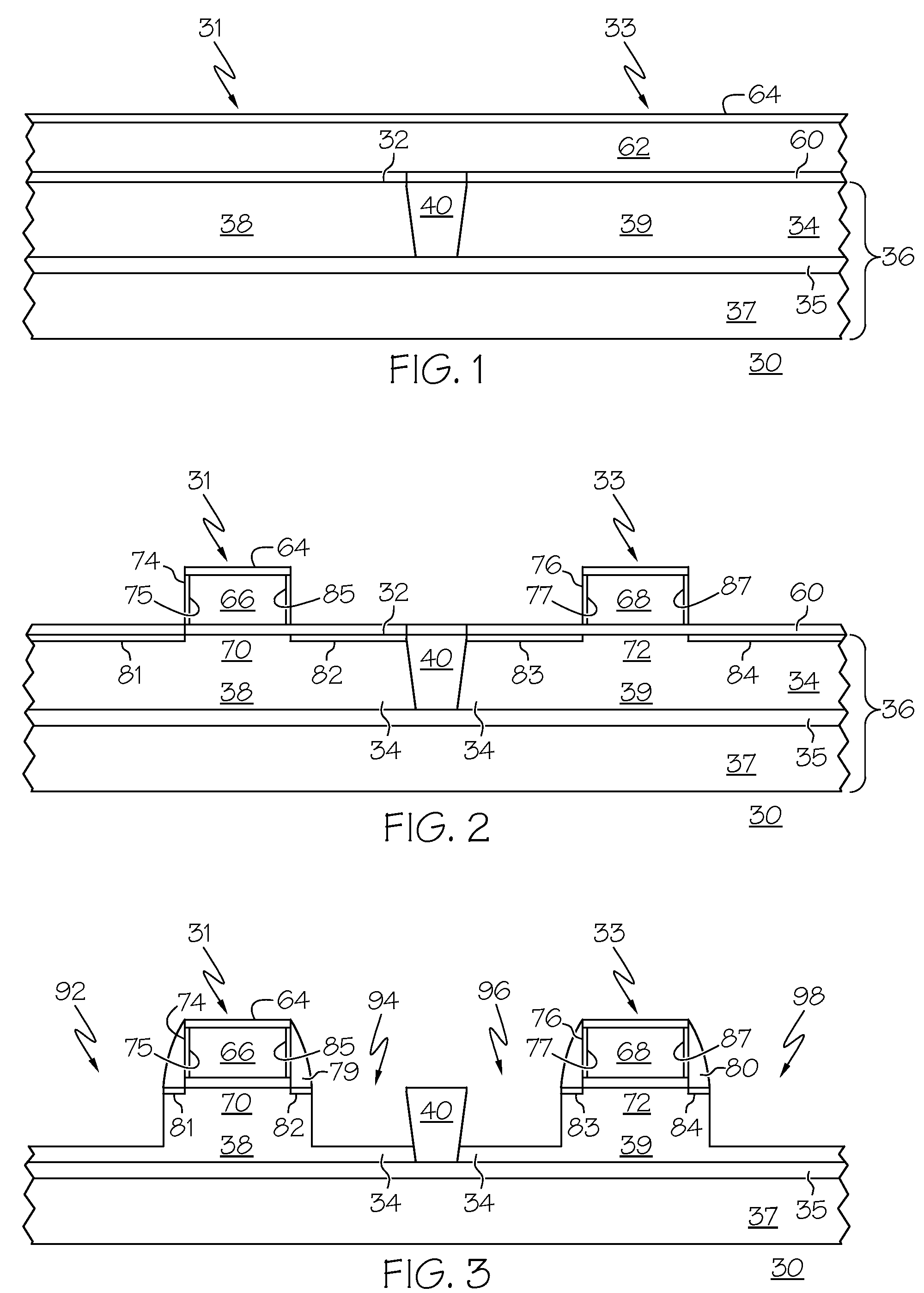
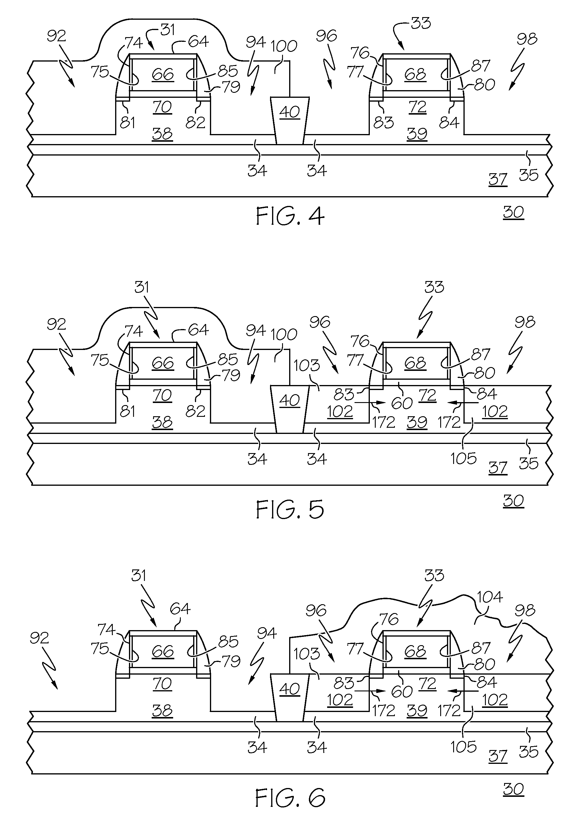
[0012]FIGS. 1-16 illustrate a stressed MOS device 30 and method steps for manufacturing such an MOS device in accordance with various embodiments. In these illustrative embodiments stressed MOS device 30 is a complementary MOS (CMOS) device here illustrated by a single NMOS transistor 31 and a single PMOS transistor 33. As will become clear from the following description, the various embodiments are directed to the fabrication of an NMOS transistor having enhanced mobility and / or a PMOS transistor that also has enhanced mobility to achieve a semiconductor device having superior on resistance characteristics. Those of skill in the art will ...


PUM


Abstract

A strain enhanced semiconductor device and methods for its fabrication are provided. One method comprises embedding a strain inducing semiconductor material in the source and drain regions of the device to induce a strain in the device channel. Thin metal silicide contacts are formed to the source and drain regions so as not to relieve the induced strain. A layer of conductive material is selectively deposited in contact with the thin metal silicide contacts, and metallized contacts are formed to the conductive material.

Description

TECHNICAL FIELD[0001]The present invention generally relates to strain enhanced semiconductor devices and to methods for their fabrication, and more particularly relates to semiconductor devices having strain inducing embedded regions and to methods for fabricating such devices without causing the strain to be relieved.BACKGROUND[0002]The majority of present day integrated circuits (ICs) are implemented by using a plurality of interconnected field effect transistors (FETs), also called metal oxide semiconductor field effect transistors (MOSFETs), or simply MOS transistors. A FET includes a gate electrode as a control electrode and spaced apart source and drain electrodes between which a current can flow. A control voltage applied to the gate electrode controls the flow of current through a channel between the source and drain electrodes.[0003]An important parameter associated with MOS transistors is the device resistance (“on resistance”) from source to drain when the device is turn...

Claims


Application Information

Patent Timeline
IPC IPC(8): H01L21/8238H01L29/94
CPCH01L21/823807H01L21/823814H01L29/517H01L29/66636H01L29/7833H01L29/7843H01L2924/0002H01L29/7848Y10S438/938H01L2924/00H01L21/32051
Inventor PAN, JAMES N.SUN, SEY-PINGWAITE, ANDREW M.
Owner ADVANCED MICRO DEVICES INC
Why Eureka
Try Eureka