Semiconductor devices and manufacturing techniques for reduced aspect ratio of neighboring gate electrode lines

a technology of semiconductor devices and gate electrodes, applied in semiconductor devices, diodes, electrical apparatus, etc., can solve the problems of reducing performance and yield loss, and the probability of contact failure, and achieve the effects of improving current drive capabilities of respective transistors, reducing the probability of contact failure, and positive influence of charge carrier mobility

Inactive Publication Date: 2019-02-07
GLOBALFOUNDRIES US INC
View PDF2 Cites 0 Cited by
  • Summary
  • Abstract
  • Description
  • Claims
  • Application Information

AI Technical Summary

Benefits of technology

[0004]Although the ongoing scaling of the semiconductor devices may contribute to enhanced performance and increased integration density, there are also certain side effects associated with the ever-decreasing critical dimensions, which may have to be addressed in order to not unduly offset some of the advantageous effects of the device scaling. Hence, a plurality of additional mechanisms are typically implemented in the overall process flow in an attempt to further enhance transistor performance without significantly contributing to additional process complexity.
[0005]A very efficient mechanism in this sense is the introduction of stress or strain into certain portions of a transistor element in order to positively influence the charge carrier mobility. Although many different approaches have been developed over the past years, which may involve the incorporation of semiconductor compounds of different lattice constants and the like, in other well-established approaches, so-called “stress liners,” i.e., material layers inducing a specific type of strain in certain transistor areas, may be applied, thereby achieving superior performance by increasing current drive capabilities of the respective transistors. One well-established approach in this context is the formation of respective strain-inducing material layers during the formation of a contact level, i.e., a device level in which respective dielectric materials are deposited over the substantially completed transistor elements in order to passivate the transistor elements and form appropriate contact elements, so as to appropriately connect to a metallization system that is to be formed above a contact level. In a corresponding process regime, one or more of the dielectric materials, which may have to be provided anyway with respect to the passivation of the transistor elements, may be provided in the form of a stressed or strain-inducing material, wherein immediate contact with the underlying transistor structure may ensure high efficiency of any such mechanism. For example, silicon nitride material may be deposited so as to induce tensile or compressive strain in underlying material layers by appropriately adapting the deposition conditions and may, therefore, represent a highly efficient mechanism for enhancing charge carrier mobility in P-type and N-type transistors, respectively.
[0006]Upon depositing such performance-increasing dielectric materials above the transistor elements, it turns out, however, that, particularly in sophisticated semiconductor devices, a very sophisticated surface topography may be encountered during the deposition process, thereby possibly contributing to reduced efficiency of the strain-inducing mechanism and / or contributing to pronounced device failures, particularly in the contact level.
[0007]In view of the situation described above, the present disclosure, therefore, relates to semiconductor devices and manufacturing techniques in which resistors and sophisticated transistors may be formed so as to provide required device characteristics of the resistors and the transistors, while avoiding, or at least reducing, the effects of one or more of the problems identified above.SUMMARY OF THE DISCLOSURE
[0008]The following presents a simplified summary of the disclosure in order to provide a basic understanding of some aspects of the invention. This summary is not an exhaustive overview of the invention. It is not intended to identify key or critical elements of the invention or to delineate the scope of the invention. Its sole purpose is to present some concepts in a simplified form as a prelude to the more detailed description that is discussed later.
[0009]Generally, the present disclosure is based on the finding that, in particular, the process sequence related to defining non-silicided areas in the resistor material, resulting in respective sidewall spacers of raised drain and source regions and on gate electrode lines formed above isolation regions, may be efficiently replaced by process strategies that do not require the deposition of a respective mask material. In this manner, a significant relaxation, particularly with respect to deposition constraints during the further processing of semiconductor devices, for instance, upon depositing a dielectric material for the contact level, such as a strain-inducing dielectric material and the like, may be accomplished, thereby reducing performance and yield loss, as well as the probability of contact failures.

Problems solved by technology

In this manner, a significant relaxation, particularly with respect to deposition constraints during the further processing of semiconductor devices, for instance, upon depositing a dielectric material for the contact level, such as a strain-inducing dielectric material and the like, may be accomplished, thereby reducing performance and yield loss, as well as the probability of contact failures.

Method used


Image

  • Semiconductor devices and manufacturing techniques for reduced aspect ratio of neighboring gate electrode lines
  • Semiconductor devices and manufacturing techniques for reduced aspect ratio of neighboring gate electrode lines
  • Semiconductor devices and manufacturing techniques for reduced aspect ratio of neighboring gate electrode lines

Examples


Embodiment Construction

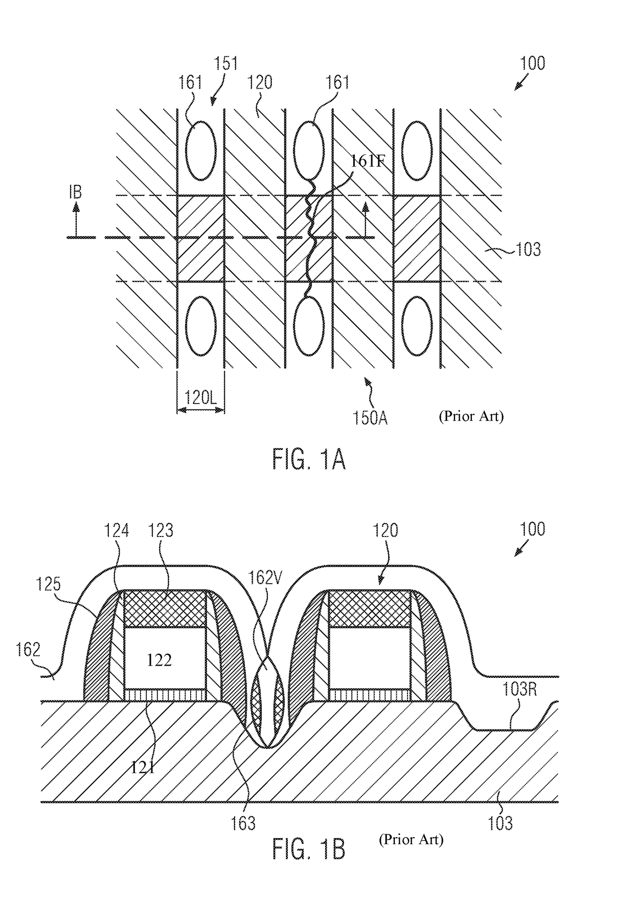
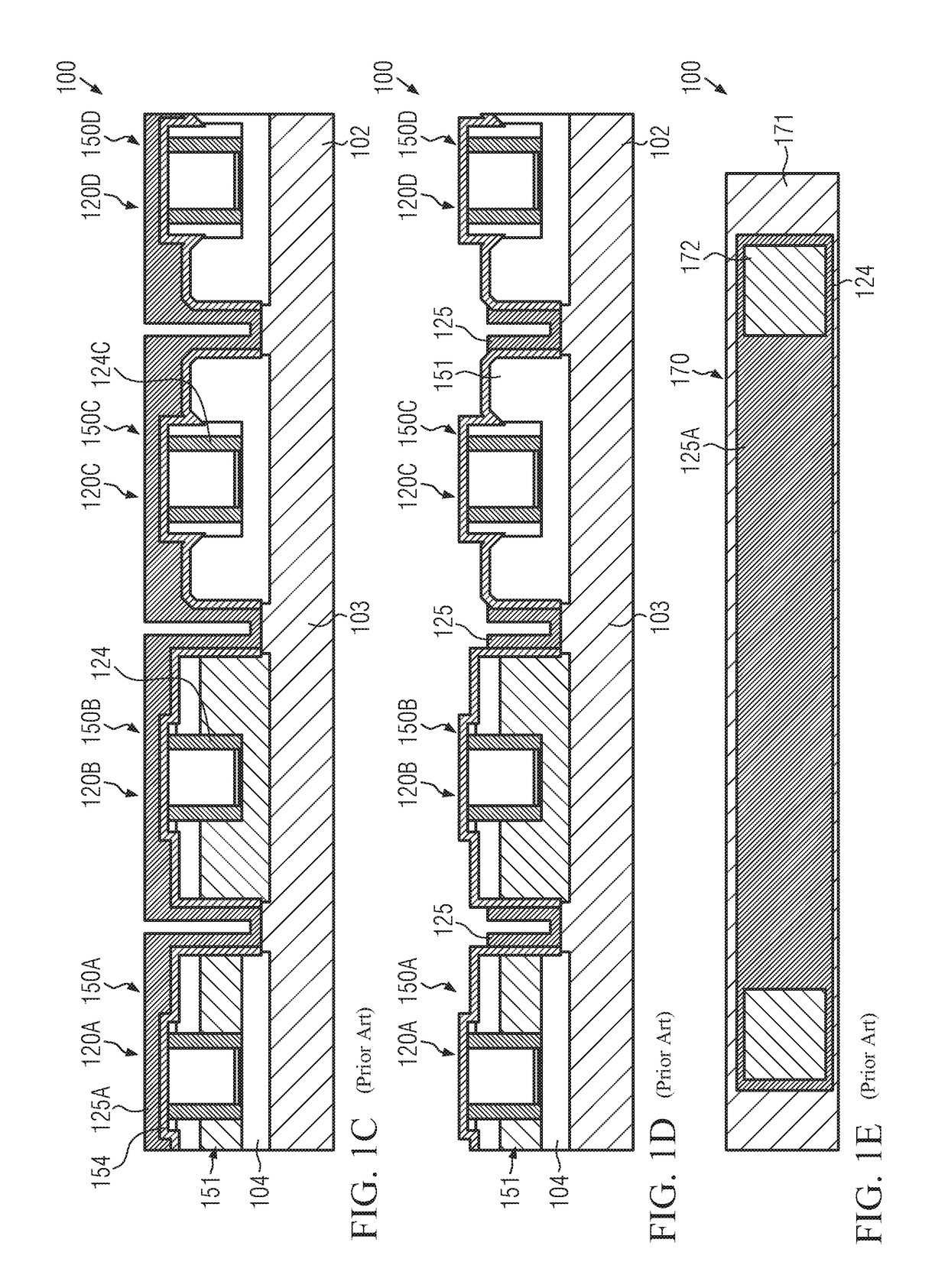
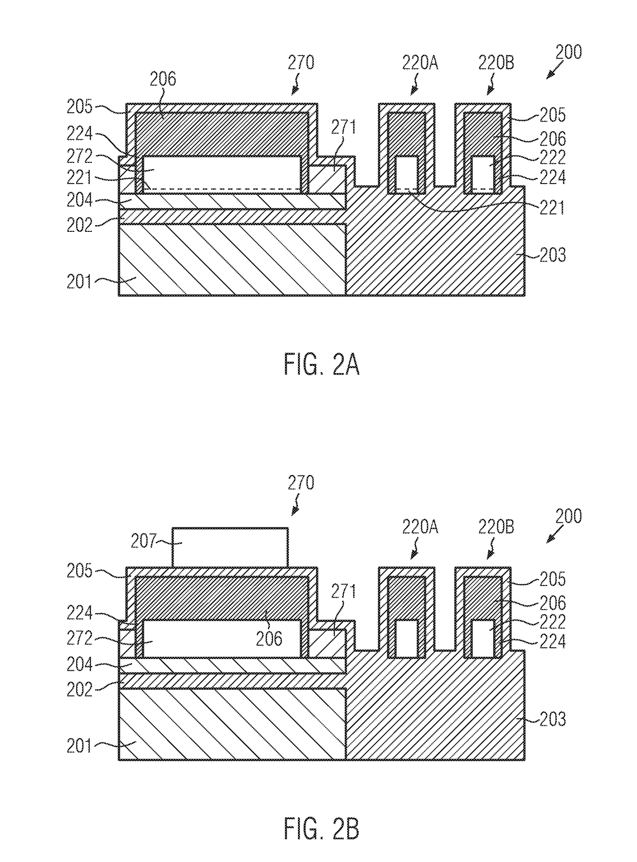
[0021]In the following description, for the purposes of explanation, numerous specific details are set forth in order to provide a thorough understanding of exemplary embodiments. It should be apparent, however, that exemplary embodiments may be practiced without these specific details or with an equivalent arrangement. In other instances, well-known structures and devices are shown in block diagram form in order to avoid unnecessarily obscuring exemplary embodiments. In addition, unless otherwise indicated, all numbers expressing quantities, ratios and numerical properties of ingredients, reaction conditions and so forth used in the specification and claims are to be understood as being modified in all instances by the term “about.”

[0022]Various illustrative embodiments of the invention are described below. In the interest of clarity, not all features of an actual implementation are described in this specification. It will of course be appreciated that in the development of any suc...


PUM


Abstract

When forming sophisticated semiconductor devices requiring resistors based on polysilicon material having non-silicided portions, the respective cap material for defining the silicided portions may be omitted during the process sequence, for instance, by using a patterned liner material or by applying a process strategy for removing the metal material from resistor areas that may not receive a corresponding metal silicide. By implementing the corresponding process strategies, semiconductor devices may be obtained with reduced probability of contact failures, with superior performance due to relaxing surface topography upon forming the contact level, and / or with increased robustness with respect to contact punch-through.

Description

BACKGROUND1. Field of the Disclosure[0001]Generally, the present disclosure relates to semiconductor devices and manufacturing techniques in which passive-resistive structures may be provided in complex integrated circuits, including sophisticated transistor elements with raised drain and source architecture in combination with closely spaced gate electrode lines.2. Description of the Related Art[0002]Significant progress has been made in the field of semiconductor devices, typically including active circuit elements, such as transistors in the form of sophisticated field effect transistors, i.e., transistors comprising drain and source regions and a gate electrode structure. Depending on the overall complexity of a circuit configuration of interest, these transistor elements may be formed on the basis of critical dimensions of 30 nm and even less in sophisticated planar transistor architectures, thereby providing the potential to achieve extremely high integration density, thus off...

Claims


Application Information

Patent Timeline
Patent Type & Authority Applications(United States)
IPC IPC(8): H01L21/84H01L27/06H01L49/02H01L29/06H01L29/08H01L29/78H01L27/12
CPCH01L21/84H01L27/0629H01L28/20H01L29/7843H01L29/0847H01L29/7838H01L27/1203H01L29/0649H01L21/823412H01L21/823468H01L27/13H01L29/66628H01L29/665
Inventor MOLL, HANS-PETERBAARS, PETERGRASSHOFF, GUNTER
Owner GLOBALFOUNDRIES US INC
Why Eureka
Try Eureka