Phase-Change Memory Device

a phase-change memory and phase-change technology, applied in the direction of bulk negative resistance effect devices, solid-state devices, instruments, etc., can solve the problems of difficult to maintain the characteristics and increase the complexity of cell array configuration

Inactive Publication Date: 2008-10-23
KK TOSHIBA
View PDF4 Cites 138 Cited by
  • Summary
  • Abstract
  • Description
  • Claims
  • Application Information

AI Technical Summary

Benefits of technology

[0009]A phase-change memory device in accordance with another embodying mode of this invention has an insulative substrate, a plurality of first wiring lines formed in parallel with each other above the insulative substrate, memory cells being formed over each the first wiring line so that one end is connected to each the first wiring line, each the memory cell having a stacked structure of a variable resistive element and a diode, the variable resistive element storing as information a resistance value determined due to phase-change between crystalline and amorphous states thereof, and a plurality of second wiring lines formed over the memory cells to commonly connect together the other end portions of the memory cells arrayed in a direction crossing the first wiring lines.
[0010]A phase-change memory device in accordance

Problems solved by technology

If no wiring lines other than these row/column select lines are formed, then the cell array becomes simpler in configuration; however, in the prior art semiconductor memories, the cell array has been configured with increased complexities

Method used


Image

  • Phase-Change Memory Device
  • Phase-Change Memory Device
  • Phase-Change Memory Device

Examples


Embodiment Construction

[0088]An explanation will be given of embodiments of this invention below.

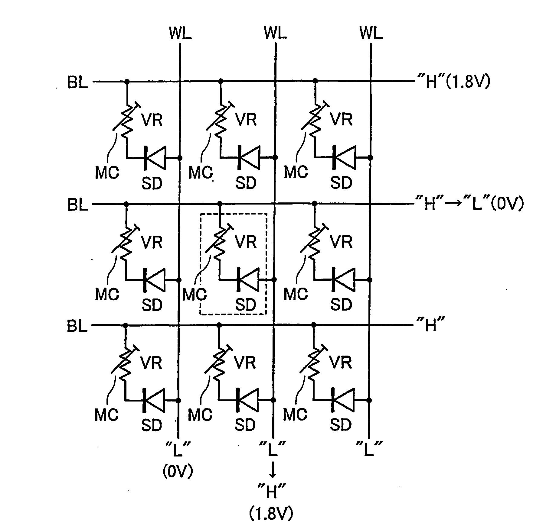
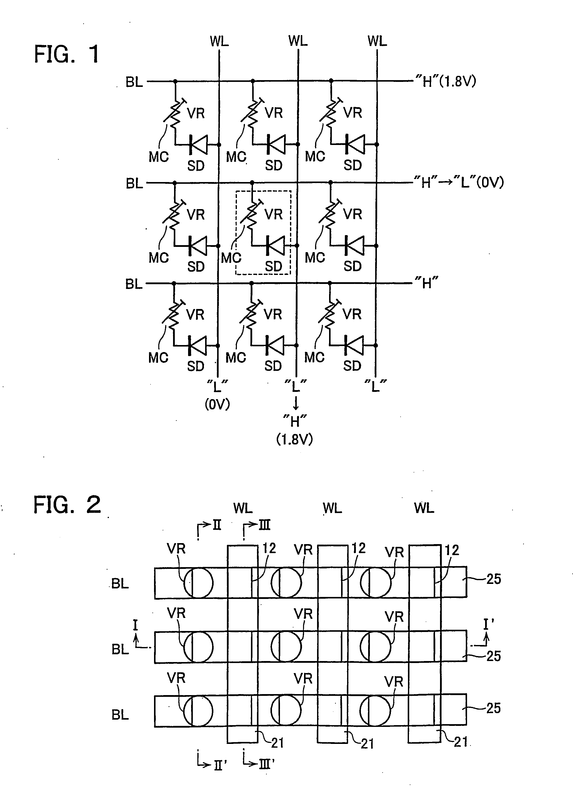
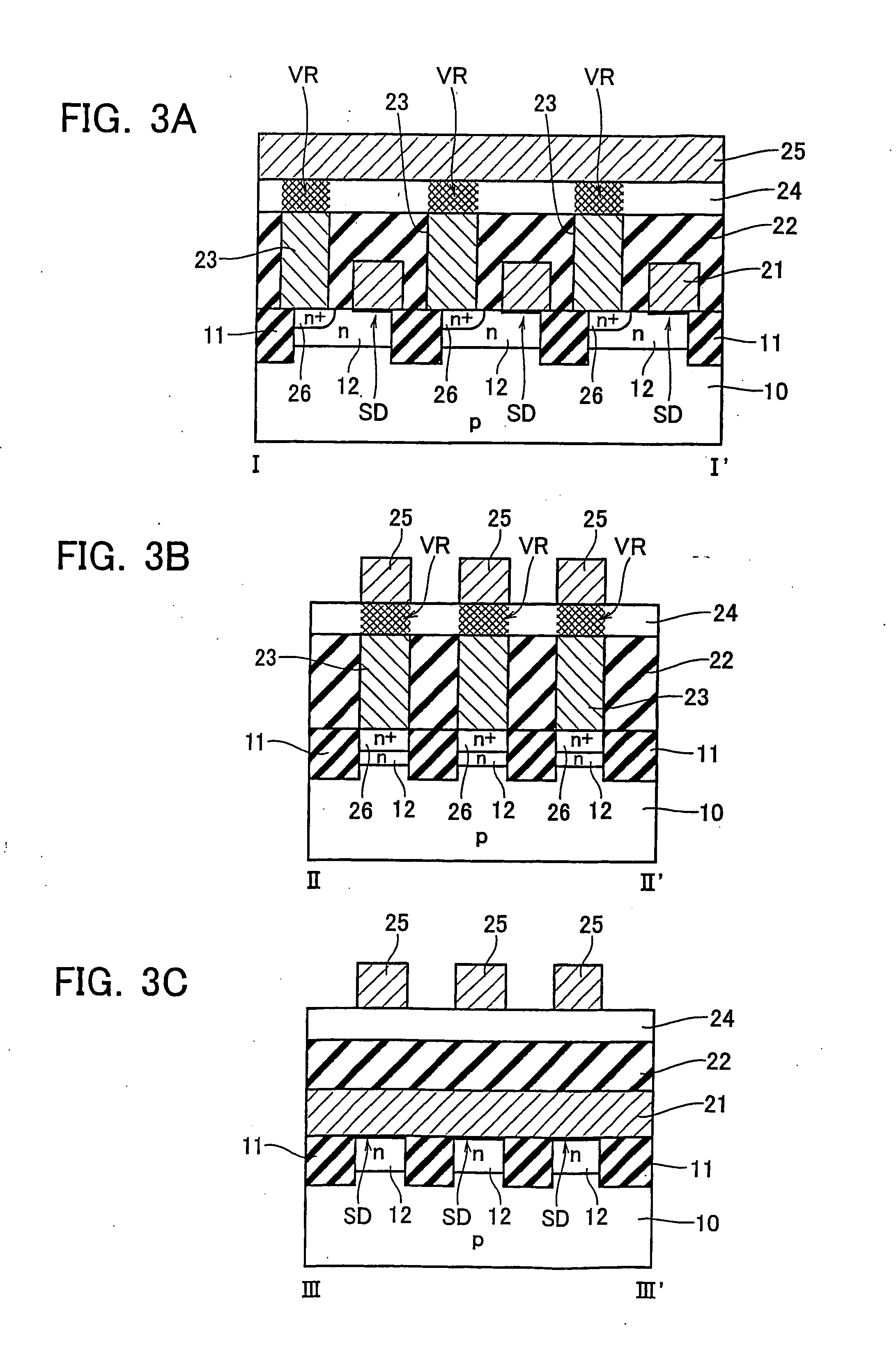
[0089]FIG. 1 shows a cell array of a phase-change memory in accordance with an embodiment, with respect to a 3×3 cell matrix. A plurality of first wiring lines (referred to as word lines hereinafter) WL are provided in parallel, and a plurality of second wiring lines (referred to hereinafter as bit lines) BL are provided to cross over the first lines. Memory cells MC are laid out at the respective crossing points of these lines. The memory cell MC is a series-connection circuit of a variable resistive element VR and a diode SD. The variable resistive element VR is formed of chalcogenide and is operable to store therein a resistance value determined due to a phase transition between its crystalline and amorphous states as information in a nonvolatile manner.

[0090]Although the diode SD is a Schottky diode in the case of this embodiment, a pn-junction diode is alternatively usable. One end of the memory cell MC i...


PUM


Abstract

A phase-change memory device has a plurality of first wiring lines WL extending in parallel to each other, a plurality of second wiring lines BL which are disposed to cross the first wiring lines WL while being separated or isolated therefrom, and memory cells MC which are disposed at respective cross points of the first wiring lines WL and the second wiring lines BL and each of which has one end connected to a first wiring line WL and the other end connected to a second wiring line BL. The memory cell MC has a variable resistive element VR which stores as information a resistance value determined due to phase change between crystalline and amorphous states thereof, and a Schottky diode SD which is connected in series to the variable resistive element VR.

Description

TECHNICAL FIELD[0001]This invention relates to an electrically rewritable phase-change memory device (ovonic memory device) which stores a resistance value determined due to a phase change between crystalline and amorphous states of a memory material as information in a non-volatile manner.BACKGROUND ART[0002]Prior known electrically rewritable semiconductor memory devices are generally categorized into volatile memories and nonvolatile memories. Whereas volatile memories include DRAMs and SRAMs, nonvolatile memories include EEPROM flash memories such as those of the NAND or NOR type or the like. The DRAMs and SRAMs are featured by high-speed random accessibility; the flash memories feature large capacity and long-term data retainability. The ones with nonvolatility which are capable of offering high-speed random accessibility also include ferro-electric RAMs using ferroelectric films. In these prior art semiconductor memories, they must have, without fail, transistors for use as th...

Claims


Application Information

Patent Timeline
IPC IPC(8): H01L25/03G11C11/21H01L21/8239G11C13/00G11C11/34G11C11/56G11C16/02G11C16/10G11C16/28H01L27/105H01L45/00
CPCG11C11/56G11C11/5678G11C13/0004G11C13/003G11C13/004G11C13/0069G11C2013/0054G11C2013/009G11C2213/71G11C2213/72G11C2213/78G11C2213/79H01L45/06H01L45/1233H01L27/2409H01L27/2472H01L27/2481H10B63/82H10B63/84H10B63/20H10N70/231H10N70/826
Inventor TODA, HARUKI
Owner KK TOSHIBA
Why Eureka
Try Eureka