Liquid crystal display apparatus, method of controlling the same, and liquid crystal projector system

a technology of liquid crystal display and display circuit, which is applied in the direction of static indicating devices, non-linear optics, instruments, etc., can solve the problems of excessive load of output circuit and damage to output circuit, and achieve the effect of preventing the reduction of lifespan

Inactive Publication Date: 2008-10-23
CANON KK
View PDF8 Cites 9 Cited by
  • Summary
  • Abstract
  • Description
  • Claims
  • Application Information

AI Technical Summary

Benefits of technology

[0013]According to the present invention, the output of the image signal generating circuit does not become short circuited with a reference voltage. Accordingly, without damaging the image signal generating circuit, voltages stored at pixels can be discharged quickly. This serves to prevent reduction of lifespan (reliability).

Problems solved by technology

However, Japanese Patent Laid-Open No. 2004-226597 does not make clear the relationship between the discharging signal and the state of selector switches (hereinafter referred to as transferring switches) that connect the signal lines with a driver circuit (source driver) for driving the signal lines.
This causes an excessive load of the output circuit of the source driver (i.e., an excessive current flows), possibly causing damage to the output circuit.

Method used


Image

  • Liquid crystal display apparatus, method of controlling the same, and liquid crystal projector system
  • Liquid crystal display apparatus, method of controlling the same, and liquid crystal projector system
  • Liquid crystal display apparatus, method of controlling the same, and liquid crystal projector system

Examples


first embodiment

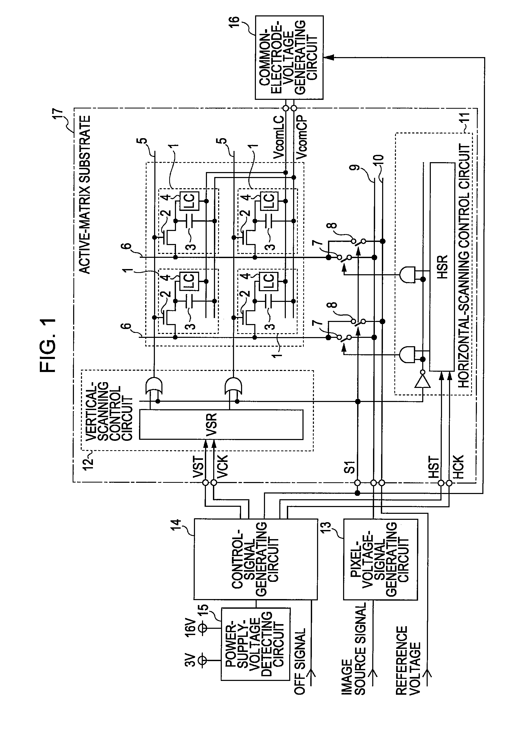
[0021]FIG. 1 is a diagram showing an example configuration of a liquid crystal display apparatus according to a first embodiment of the present invention. Referring to FIG. 1, a display area is formed of unit pixels 1. Each of the pixels 1 is formed of a pixel transistor 2 that serves as a switching element, a pixel storage capacitor 3, and a liquid crystal 4. A counter electrode of the pixel storage capacitors 3 is formed commonly for all the pixels 1. Although not shown, an electrode is provided at an end where the pixel transistor 2 and the pixel storage capacitor 3 are connected to each other, and the liquid crystal 4 is disposed between the electrode and an electrode provided commonly for all the pixels 1 (usually formed of a transparent electrode).

[0022]The counter electrode of the pixel storage capacitor 3 and the common electrode holding the liquid crystal 4, described above, are both connected to a common electrode voltage generating circuit 16 provided outside an active ma...

second embodiment

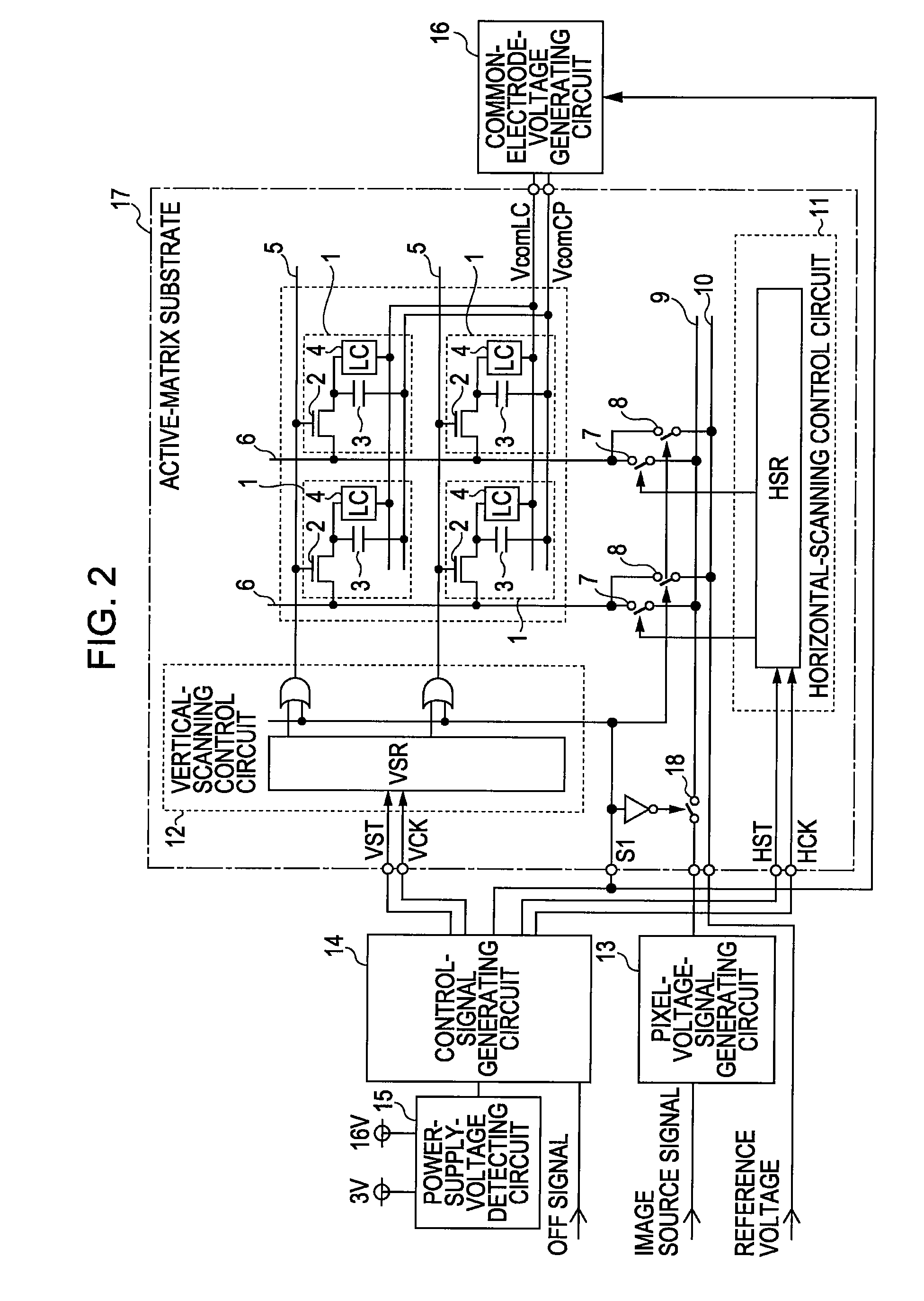
[0038]FIG. 2 is a diagram showing an example configuration of a liquid crystal display apparatus according to a second embodiment of the present invention. The configurations of the pixels 1, the vertical scanning control circuit 12, the gate lines 5, and the circuits provided outside the active matrix substrate 17 are the same as those in the first embodiment, so that description thereof will be omitted. The following description will be directed mainly to configurations of parts that differ from parts in the first embodiment.

[0039]A main difference with the configuration of the first embodiment is that a third switch (hereinafter referred to as a disconnecting switch) 18 is provided between the transferring switches 7 and the pixel voltage signal generating circuit 13. The control terminal of the disconnecting switch 18 receives input of the control signal S1 through the inverter circuit. The control signal S1 is a signal output from the control signal generating circuit 14.

[0040]...

third embodiment

[0048]FIG. 3 is a diagram showing an example configuration of a liquid crystal display apparatus according to a third embodiment of the present invention. Since the configurations of the pixels 1, the vertical scanning control circuit 12, the gate lines 5, and the circuits provided outside the active matrix substrate 17 are the same as those in the first embodiment, description thereof will be omitted. The following description will be directed mainly to the configurations of parts that differ from parts in the first embodiment.

[0049]Each of the signal lines 6 is connected to a first switch (hereinafter referred to as a transferring switch) 7, and the other end of the transferring switch 7 is connected to a video line 9 that transmits pixel voltage signals. The video line 9 is connected to a second switch (hereinafter referred to as a discharging switch) 8 and a third switch (hereinafter referred to as a disconnecting switch) 18.

[0050]The other end of the discharging switch 8 is con...


PUM

PropertyMeasurementUnit
voltageaaaaaaaaaa
voltageaaaaaaaaaa
voltageaaaaaaaaaa

Abstract

A liquid crystal display apparatus includes a display area in which pixels each having a switching element and electrode are arranged forming a matrix; a first scanning circuit to control whether the switching elements are turned on or off via first wires; a second scanning circuit to control whether an image signal generating circuit is electrically connected to or disconnected from second wires, and to assign image signals to the pixels via those wires; a discharging element to discharge the assigned image signals; a detecting circuit to detect reduction in a power supply voltage and to output a detection signal; and a control circuit to perform a controlling operation according to the signal so that the image signal generating circuit is electrically disconnected from the second wires, the switching elements are turned on, and the discharging element is caused to operate.

Description

BACKGROUND OF THE INVENTION[0001]1. Field of the Invention[0002]The present invention relates to liquid crystal display apparatuses, and particularly to techniques that are effective for discharging charges from pixels at the time of power-off or the like.[0003]2. Description of the Related Art[0004]In a liquid crystal display apparatus, if power is turned off with charging remaining at pixels, the liquid crystal display apparatus is left for a long period with a DC voltage applied to a liquid crystal layer. This causes image sticking, which results in reduction of the lifespan (reliability) of the liquid crystal. Therefore, at the time of power-off, charges remaining at the pixels (remaining charges) must be discharged quickly.[0005]In a first method according to the related art, in order to discharge remaining charges at the time of power off, before the liquid crystal display apparatus is powered off, a white signal (or a black signal) is written by controlling timing of writing ...

Claims


Application Information

Patent Timeline
Patent Type & Authority Applications(United States)
IPC IPC(8): G09G3/36G02F1/13
CPCG02F1/13452G09G3/3688G09G2310/0245G09G2330/02G09G2330/027
Inventor OOMURA, MASANOBUKAMEYAMA, HIROAKI
Owner CANON KK
Why Eureka
Try Eureka