Semiconductor package using copper wires and wire bonding method for the same

a technology of copper wire and semiconductor, applied in the direction of semiconductor devices, semiconductor/solid-state device details, electrical apparatus, etc., can solve the problems of non-uniform size of free air balls, ball lift problems in the fabrication process, ball lift problems, etc., to improve the bondability of copper wires and good bonding

Inactive Publication Date: 2008-10-30
SILICONWARE PRECISION IND CO LTD
View PDF1 Cites 18 Cited by
  • Summary
  • Abstract
  • Description
  • Claims
  • Application Information

AI Technical Summary

Benefits of technology

[0007]In light of the drawback associated with the conventional techniques as described above, an objective of the present invention is to provide a semiconductor package using copper wires and a wire bonding method for the same, which enhances bondability of copper wires on fingers of a carrier by implanting on the fingers of the carrier Au stud bumps that have good bonding with the copper wires, thereby overcoming the stitch lift problem of the prior art.

Problems solved by technology

Due to high cost of gold, however, there is a trend in the art to migrate from using gold wires to using other materials such as Copper (Cu).
But copper cannot form good bonding with the silver-coated layer on the fingers of a leadframe or the Ni / Au layer on the fingers of a substrate, which thus may lead to short tail of the stitch ends of copper wires bonded to the fingers and further lead to uneven tail ends and inconsistent tail length of copper wires remained beyond the capillary after a bonding process, thus adversely affecting formation of free air balls (FAB) for a subsequent wire bonding process and resulting in nonuniform size of free air balls.
Nonuniform size of the free air balls can easily result in poor bonding between the free air balls and the bond pads of the chip, thus adversely and ultimately causing a ball lift problem in the fabrication process.
As a result, the free air balls 302′ of different sizes are formed before subsequent wire-bonding process, which easily results in ball lift problem of the free air balls 302′ bonded to the bond pads 330′ of the chip 33′.
However, the problems of stitch lift or short tail of the stitch ends 400 bonded to the fingers 411 still exist since the copper wire 40 cannot form good bonding with the silver-coated layer or the Ni / Au layer formed on the fingers 411 of a leadframe or a substrate 41, which further adversely affects uniformity of the free air balls to be formed subsequently.

Method used


Image

  • Semiconductor package using copper wires and wire bonding method for the same
  • Semiconductor package using copper wires and wire bonding method for the same
  • Semiconductor package using copper wires and wire bonding method for the same

Examples


Embodiment Construction

[0019]The present invention is described in the following with specific embodiments, so that one skilled in the pertinent art can easily understand other advantages and effects of the present invention from the disclosure of the invention. The present invention may also be implemented and applied according to other embodiments, and the details may be modified based on different views and applications without departing from the spirit of the invention.

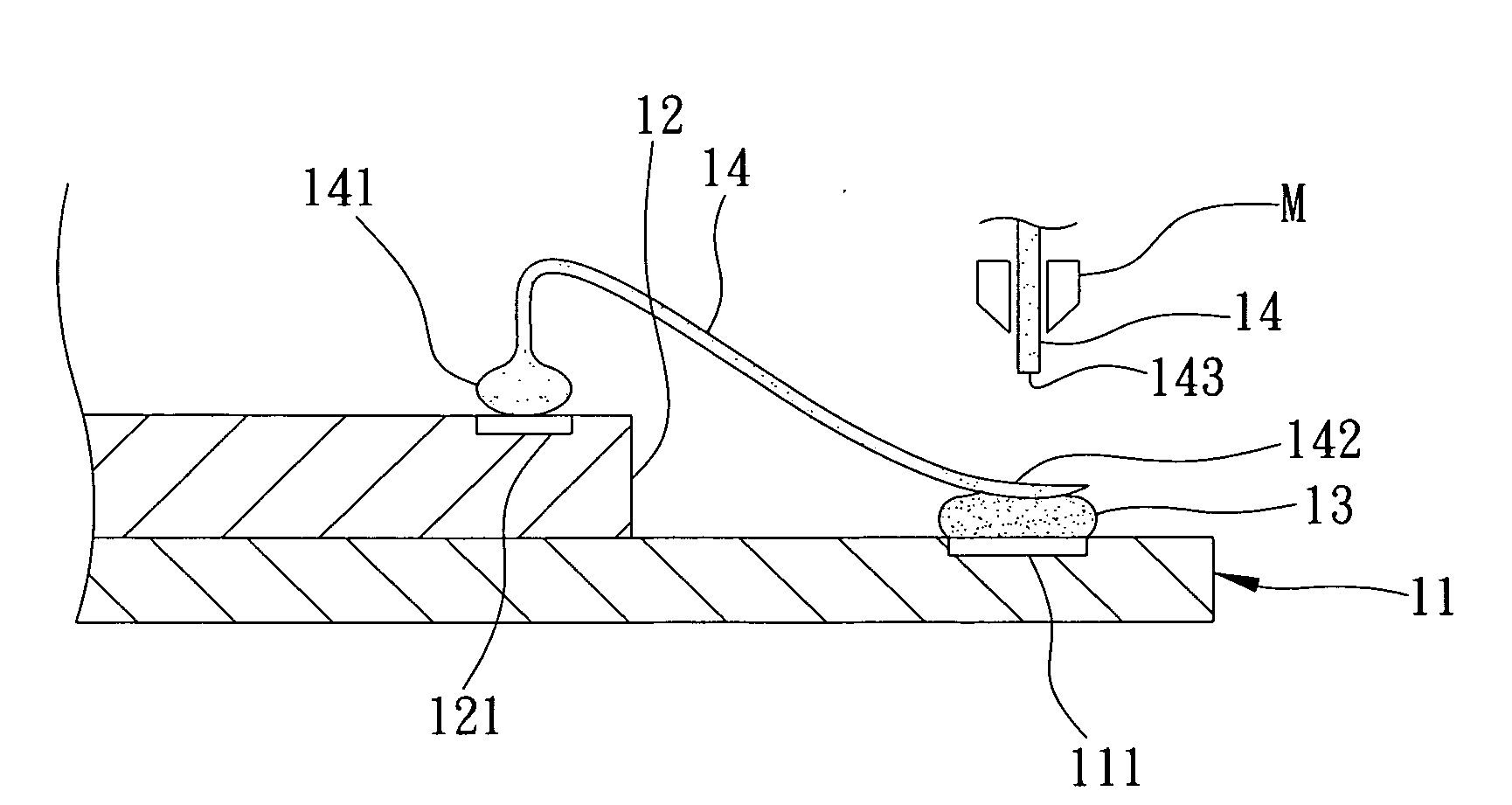
[0020]FIG. 1 illustrates a semiconductor package using Cu wires according to the present invention, which comprises a substrate 11, a chip 12 mounted on the substrate 11, a plurality of Au stud bumps 13 implanted on the substrate 11, a plurality of copper wires 14 for electrically connecting the substrate 11 and the chip 12, and an encapsulant 15 formed on the substrate 11 for encapsulating the chip 12, the Au stud bumps 13 and the copper wires 14.

[0021]The substrate 11 has a plurality of fingers 111 formed thereon such that the Au stud...


PUM


Abstract

A semiconductor package using copper wires and a wire bonding method for the same are proposed. The package includes a carrier having fingers and a chip mounted on the carrier. The method includes implanting stud bumps on the fingers of the carrier and electrically connecting the chip and the carrier by copper wires with one ends of the copper wires being bonded to bond pads of the chip and the other ends of the copper wires being bonded to the stud bumps on the carrier. The implanted stud bumps on the carrier improve bondability of the copper wires to the carrier and thus prevent stitch lift. With good bonding, residues of copper wires left behind after a bonding process have even tail ends and uniform tail length to enable fabrication of solder balls of uniform size, thereby eliminating a conventional step of implanting stud bumps on the bond pads of chips and preventing ball lift from occurring.

Description

FIELD OF THE INVENTION[0001]The invention relates to a semiconductor package and a wire bonding method for the same. More particularly, the invention relates to a semiconductor package using copper wires for electrically connecting a carrier to a chip mounted on the carrier and a wire bonding method for the same.BACKGROUND OF THE INVENTION[0002]In conventional semiconductor packages, gold wires are generally used to electrically connect a chip to a chip carrier such as a leadframe or a substrate, since gold wires can form good bonding with a silver-coated layer on fingers of the leadframe or a Ni / Au layer on fingers of the substrate, a good bonding quality between the gold wires and the fingers can be ensured. Due to high cost of gold, however, there is a trend in the art to migrate from using gold wires to using other materials such as Copper (Cu). But copper cannot form good bonding with the silver-coated layer on the fingers of a leadframe or the Ni / Au layer on the fingers of a s...

Claims


Application Information

Patent Timeline
Patent Type & Authority Applications(United States)
IPC IPC(8): H01L21/60H01L23/495
CPCH01L23/49811H01L24/45H01L24/48H01L24/78H01L24/85H01L2224/45144H01L2224/45147H01L2224/48091H01L2224/48227H01L2224/48247H01L2224/4845H01L2224/48465H01L2224/48475H01L2224/4848H01L2224/48482H01L2224/48499H01L2224/48599H01L2224/78301H01L2224/85051H01L2224/85181H01L2224/85205H01L2224/85986H01L2924/01028H01L2924/01029H01L2924/01047H01L2924/01079H01L2924/01082H01L2924/014H01L2924/09701H01L2924/00014H01L2924/01033H01L2924/00H01L2924/00015H01L2924/15787H01L2924/181H01L2224/85444H01L2224/85455H01L23/4952H01L2924/00012H01L2224/4554
Inventor TSAI, HAN-LUNGHUANG, CHIH-MINGHSIAO, CHENG-HSU
Owner SILICONWARE PRECISION IND CO LTD
Why Eureka
Try Eureka