Highly Reliable Low Cost Structure for Wafer-Level Ball Grid Array Packaging

a grid array and high-reliability technology, applied in the direction of electrical equipment, semiconductor devices, semiconductor/solid-state device details, etc., can solve the problems of high cost of two polymer layers present in a bga package, difficult to implement wafer-level bga package technology, etc., and achieve the effect of fewer manufacturing process steps

Inactive Publication Date: 2008-10-30
AVAGO TECH WIRELESS IP SINGAPORE PTE
View PDF19 Cites 35 Cited by
  • Summary
  • Abstract
  • Description
  • Claims
  • Application Information

AI Technical Summary

Benefits of technology

[0009]In another aspect, a single insulating layer is used to provide stress absorption for stresses applied to the bump interconnect, while enabling fewer manufacturing process steps than required in multiple polymer layer configurations.

Problems solved by technology

A current move to tighter fabrication tolerances, such as 65 nm, with a continuing need to meet strict customer reliability requirements and ongoing cost pressures, is causing difficulties in implementing wafer-level BGA package technology.
However, having two polymer layers present in a BGA package is expensive.

Method used


Image

  • Highly Reliable Low Cost Structure for Wafer-Level Ball Grid Array Packaging
  • Highly Reliable Low Cost Structure for Wafer-Level Ball Grid Array Packaging
  • Highly Reliable Low Cost Structure for Wafer-Level Ball Grid Array Packaging

Examples


example embodiments

[0076]The example embodiments described herein are provided for illustrative purposes, and are not limiting. The examples described herein may be adapted to a variety of types of integrated circuit packages. Further structural and operational embodiments, including modifications / alterations, will become apparent to persons skilled in the relevant art(s) from the teachings herein.

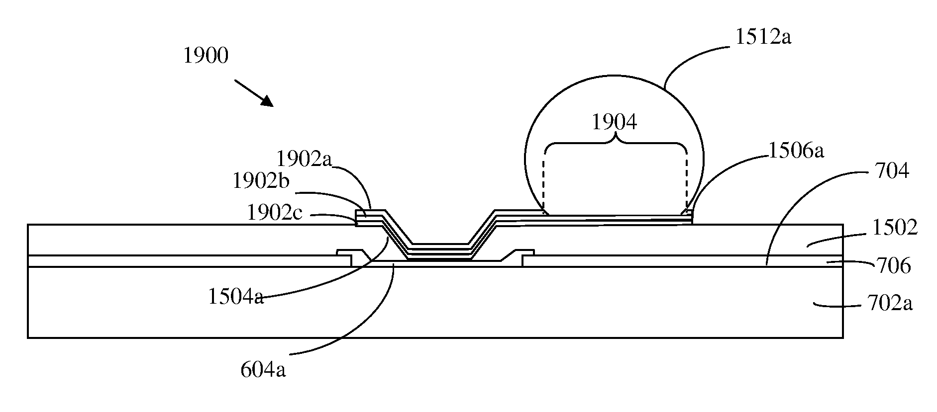
[0077]According to an embodiment, a routing interconnect for each chip terminal is used to couple the chip terminal to a bump interconnect (or other package interconnect type). In an embodiment, the routing interconnect directly connects the chip terminal to the bump interconnect. In another embodiment, an under bump metallization layer mounts the bump interconnect to the routing interconnect, and thus is also used to connect the chip terminal to the bump interconnect. In embodiments, an insulating layer between the routing interconnect and chip is used to provide stress absorption, while allowing for fewer ...


PUM


Abstract

Methods, systems, and apparatuses for wafer-level integrated circuit (IC) packages are described. An IC package includes an IC chip, an insulating layer on the IC chip, a plurality of vias, a plurality of routing interconnects, and a plurality of bump interconnects. The IC chip has a plurality of terminals configured in an array on a surface of the IC chip. A plurality of vias through the insulating layer provide access to the plurality of terminals. Each of the plurality of routing interconnects has a first portion and a second portion. The first portion of each routing interconnect is in contact with a respective terminal of the plurality of terminals though a respective via, and the second portion of each routing interconnect extends over the insulating layer. Each bump interconnect of the plurality of bump interconnects is connected to the second portion of a respective routing interconnect of the plurality of routing interconnects.

Description

BACKGROUND OF THE INVENTION[0001]1. Field of the Invention[0002]The present invention relates to integrated circuit packaging technology, and more particularly to wafer-level ball grid array packages.[0003]2. Background Art[0004]Integrated circuit (IC) chips or dies are typically interfaced with other circuits using a package that can be attached to a printed circuit board (PCB). One such type of IC die package is a ball grid array (BGA) package. BGA packages provide for smaller footprints than many other package solutions available today. A BGA package has an array of solder ball pads located on a bottom external surface of a package substrate. Solder balls are attached to the solder ball pads. The solder balls are reflowed to attach the package to the PCB.[0005]An advanced type of BGA package is a wafer-level BGA package. Wafer-level BGA packages have several names in industry, including wafer level chip scale packages (WLCSP), among others. In a wafer-level BGA package, the solde...

Claims


Application Information

Patent Timeline
Patent Type & Authority Applications(United States)
IPC IPC(8): H01L23/31H01L21/4763H01L23/50
CPCH01L23/3114H01L23/525H01L24/13H01L23/562H01L24/10H01L2224/13099H01L2224/16H01L2924/01005H01L2924/01013H01L2924/01015H01L2924/01022H01L2924/01027H01L2924/01029H01L2924/01033H01L2924/01078H01L2924/01079H01L2924/01082H01L2924/10329H01L2924/14H01L2924/01006H01L2924/01019H01L2924/01047H01L2924/014H01L2924/00H01L24/03H01L24/05H01L24/11H01L2224/0235H01L2224/05001H01L2224/05008H01L2224/05022H01L2224/05027H01L2224/051H01L2224/05569H01L2224/05572H01L2224/05611H01L2224/05624H01L2224/05639H01L2224/05644H01L2224/05647H01L2224/05655H01L2224/05666H01L2224/06131H01L2224/13H01L2224/13006H01L2224/13008H01L2224/13024H01L2224/13027H01L2224/131H01L2224/14104H01L2924/00012H01L2924/00014H01L2924/013H01L23/12H01L23/28H01L23/48
Inventor KAUFMANN, MATTHEW V.TAN, TECK YANG
Owner AVAGO TECH WIRELESS IP SINGAPORE PTE
Why Eureka
Try Eureka