Driving chip and display apparatus having the same

a technology of a display device and a driving chip, which is applied in the direction of non-linear optics, static indicating devices, instruments, etc., can solve the problems of affecting the display effect of the display device, the deviation of the resistance between the connection lines, and the display of defective images such as vertical line defects, so as to reduce the number of contacts and increase the linewidth of the connection line

Inactive Publication Date: 2008-11-06
SAMSUNG ELECTRONICS CO LTD
View PDF4 Cites 22 Cited by
  • Summary
  • Abstract
  • Description
  • Claims
  • Application Information

AI Technical Summary

Benefits of technology

[0014]According to an exemplary embodiment, the linewidth of the connection line may be increased when a resistance of the line is larger than a targeted resistance, and decreased when the resistance of the line is smaller than the targeted resistance.
[0015]According to an exemplary embodiment, the number of contacts may be decreased when a resistance of the line is larger than a targeted resistance, and increased when the resistance of the line is smaller than the targeted resistance.

Problems solved by technology

Since it is difficult to form all connection lines connecting the driving circuits and output pads to have the same length and the same configuration, resistance deviation is observed between the connection lines depending on their locations in the driving chip.
Due to the resistance deviation between the connection lines, the driving signals which are generated from the driving chip and supplied to a unit cell, are delayed or distorted, causing defective images such as a vertical line-defect to be displayed.
Even though the same pattern signal is supplied to a liquid crystal display panel, the vertical line-defect is displayed due to the resistance deviation between the connection lines.

Method used


Image

  • Driving chip and display apparatus having the same
  • Driving chip and display apparatus having the same
  • Driving chip and display apparatus having the same

Examples


Embodiment Construction

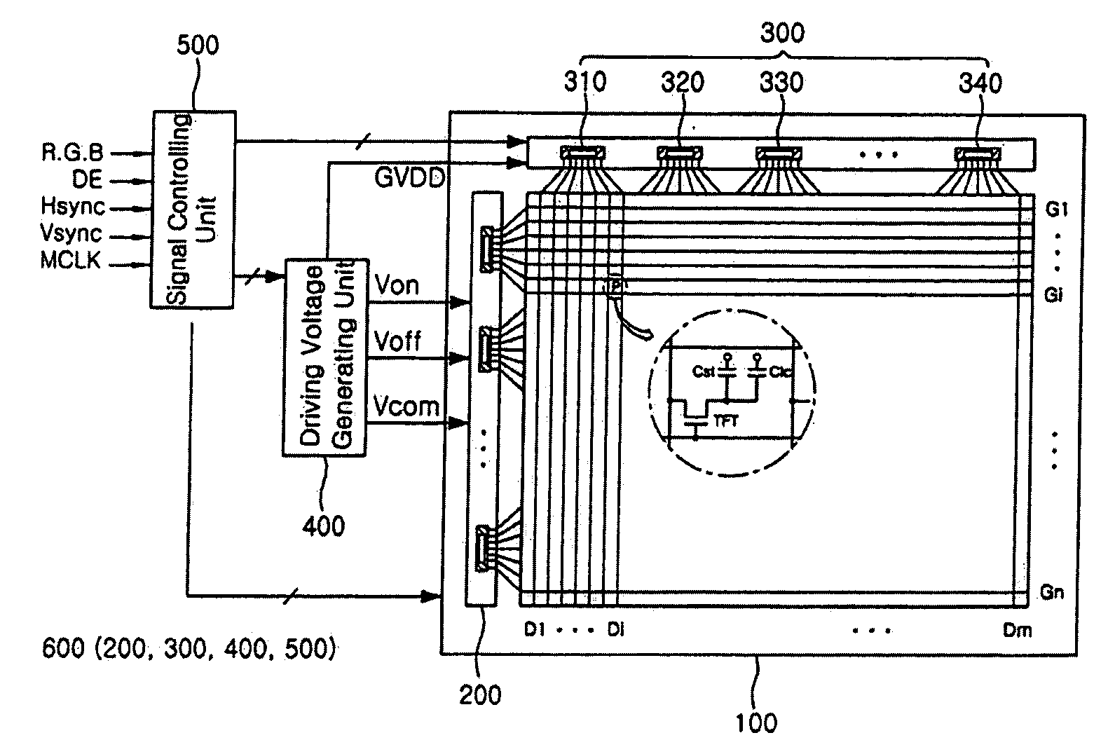
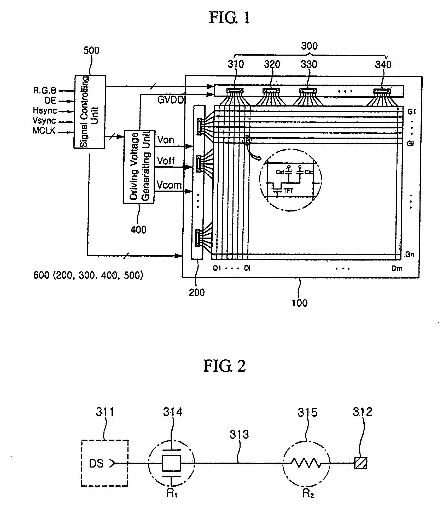
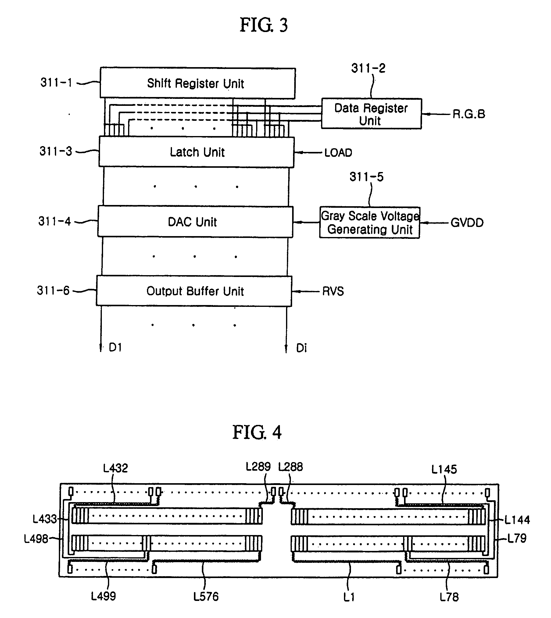
[0038]The present invention will now be described more fully hereinafter with reference to the accompanying drawings, in which embodiments of the invention are shown. This invention may, however, be embodied in many different forms and should not be construed as limited to the embodiments set forth herein. Rather, these embodiments are provided so that this disclosure will be thorough and complete, and will fully convey the scope of the invention to those skilled in the art. In the drawings, the size and relative sizes of layers and regions may be exaggerated for clarity.

[0039]It will be understood that when an element or layer is referred to as being “on,”“connected to” or “coupled to” another element or layer, it can be directly on, connected or coupled to the other element or layer or intervening elements or layers may be present. In contrast, when an element is referred to as being “directly on,”“directly connected to” or “directly coupled to” another element or layer, there are...


PUM


Abstract

A driving chip and a display apparatus having the same. The driving chip includes a plurality of driving circuits which generate a driving signal, a plurality of output pads which output the driving signals to external signal lines, a plurality of connection lines which connect the plurality of driving circuits and the plurality of output pads, respectively, wherein at least one of the plurality of connection lines includes a resistance-control unit which controls resistance values of the connection lines to be the same, and reduces a resistance deviation between the connection lines.
Thus, resistances of connection lines are controlled to be substantially the same, or resistance deviation is reduced by adjusting the resistances of the respective connection lines of an output port. Accordingly, a signal delay or a signal distortion induced by the resistance deviation of the connection lines in the driving chip is prevented, and defective images are removed.

Description

[0001]This application claims priority to Korean Patent Application No. 10-2007-0042710 filed on May 2, 2007, and all the benefits accruing therefrom under 35 U.S.C. §119, the contents of which in its entirety are herein incorporated by reference.BACKGROUND OF THE INVENTION[0002]1. Field of the Invention[0003]The invention relates to a driving chip and a display apparatus having the same, and more particularly, to a driving chip supplying a driving signal to a unit pixel and a display apparatus having the same.[0004]2. Description of the Related Art[0005]A liquid crystal display (“LCD”) displays an image by controlling a transmitted amount of light incident from a light source using optical anisotropy of liquid crystal molecules and polarization characteristic of polarizer. Recently, the application scope of LCDs is widely expanding because lightweight, slim size, high resolution, and a large screen size can be implemented in LCDs as well having low power consumption.[0006]The LCD i...

Claims


Application Information

Patent Timeline
Patent Type & Authority Applications(United States)
IPC IPC(8): G09G3/36
CPCG02F1/13452G09G3/3648G09G3/3688G09G2300/043G09G2320/0223G02F1/133G09G3/36
Inventor KIM, BORASON, SUN KYU
Owner SAMSUNG ELECTRONICS CO LTD
Why Eureka
Try Eureka